
10M16SAU169I7G Datasheet, Specifications & Application Guide – Altera MAX 10 FPGA
The 10M16SAU169I7G is a non-volatile FPGA from the Altera (Intel) MAX 10 family, built on a 55 nm flash process. It integrates 16,000 logic elements, a dual 12-bit ADC, 549 Kb of embedded SRAM, and 2,304 Kb of user flash memory into a compact 169-ball UBGA package. With single-supply operation, instant-on configuration from internal flash, and an industrial temperature rating of −40 °C to +100 °C, the 10M16SAU169I7G is engineered for cost-sensitive, space-constrained applications in industrial automation, motor control, IoT edge nodes, and mixed-signal acquisition systems.
Table of Contents
- 1. Device Overview
- 2. Key Specifications & Parameters
- 3. Functional Block Diagram
- 4. Pinout & Package Information
- 5. Typical Applications & Design Considerations
- 6. Frequently Asked Questions (FAQ)
1. Device Overview
The MAX 10 family is Altera’s (now Intel’s) single-chip, non-volatile FPGA platform that eliminates the need for external configuration flash. The 10M16SAU169I7G variant sits in the mid-range of the family, offering a balanced mix of logic density, analog capability, and I/O count in one of the smallest available packages.
The part number decodes as follows: 10M16 = MAX 10, 16K logic elements; S = single power supply; A = analog block (ADC) enabled; U169 = 169-ball UBGA package; I = industrial temperature range; 7 = speed grade 7.
Key differentiators over competing low-cost FPGAs include the integrated dual 12-bit 1 MSPS ADC that removes the need for an external converter in many sensor-interface designs, and the dual-image flash configuration that supports fail-safe remote update. The device is supported by the free Intel Quartus Prime Lite Edition toolchain, which provides synthesis, place-and-route, timing analysis, and JTAG/SPI programming.
2. Key Specifications & Parameters
| Parameter | Value |
|---|---|
| Manufacturer | Altera (Intel) |
| Family | MAX 10 (10M16) |
| Process Node | 55 nm Flash |
| Logic Elements (LEs) | 16,000 |
| Logic Array Blocks (LABs) | 1,000 |
| Embedded SRAM | 549 Kb (M9K blocks) |
| User Flash Memory (UFM) | 2,304 Kb |
| 18 × 18 Multipliers | 45 |
| PLLs | 4 |
| ADC | Dual 12-bit, up to 1 MSPS |
| Max User I/O | 130 |
| LVDS Pairs | Up to 22 |
| Package | 169-ball UBGA (11 × 11 mm, 0.8 mm pitch) |
| Core Supply Voltage | 1.2 V |
| I/O Supply Voltage | 3.0 V – 3.3 V (single supply) |
| Temperature Range | −40 °C to +100 °C (Industrial) |
| Speed Grade | 7 |
| Configuration | Internal flash, dual-image support |
| External Memory Support | DDR3, DDR2, LPDDR2, SRAM |
| I/O Standards | LVTTL, LVCMOS, SSTL, HSTL, LVDS, RSDS, Mini-LVDS |
3. Functional Block Diagram
The MAX 10 architecture arranges logic array blocks, M9K embedded memory, DSP multiplier blocks, and PLLs around a central routing fabric. The dual 12-bit ADC connects directly to dedicated analog input pins, while the user flash memory (UFM) provides on-chip non-volatile storage for calibration data or soft-processor code. Four PLLs support clock synthesis and management up to 500 MHz.
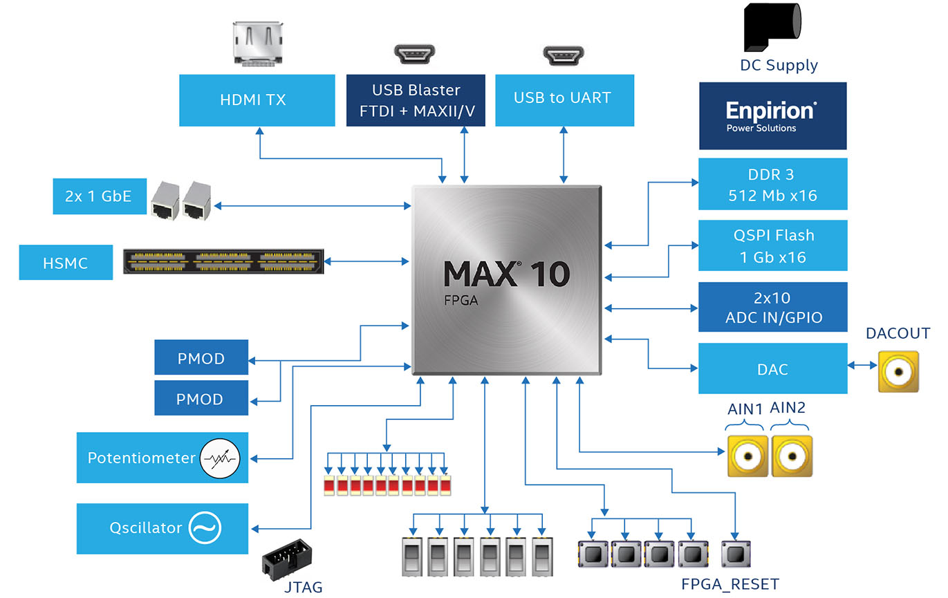
Figure 1 – MAX 10 FPGA Development Kit block diagram showing the device architecture and peripheral interfaces.
4. Pinout & Package Information
The 10M16SAU169I7G is housed in a 169-ball Ultra-thin Ball Grid Array (UBGA) measuring 11 × 11 mm with a 0.8 mm ball pitch. The package provides 130 user I/O pins organized across multiple I/O banks, each independently configurable for voltage levels from 1.2 V LVCMOS to 3.3 V LVTTL. Differential I/O pairs support LVDS signaling for high-speed serial links.
For PCB layout, the UBGA package requires a minimum of 4-layer stackup with controlled impedance for differential pairs. Altera recommends 100 Ω differential impedance for LVDS traces and provides detailed land-pattern guidelines in the device handbook. CAD symbols, footprints, and 3D STEP models are available from SnapEDA.
Figure 2 – 10M16SAU169I7G in the 169-ball UBGA package.
5. Typical Applications & Design Considerations
The combination of integrated ADC, non-volatile configuration, and a compact BGA package makes the 10M16SAU169I7G well-suited for:
- Industrial Automation & Motor Control – Real-time sensor acquisition via the dual ADC, PWM generation through FPGA logic, and fail-safe configuration for mission-critical environments.
- IoT Edge & Sensor Hubs – Instant-on boot from internal flash eliminates external configuration memory, reducing BOM cost and board area. The UFM stores calibration coefficients and firmware images.
- Communications & Protocol Bridging – 45 embedded multipliers handle DSP-intensive tasks such as digital filtering and modulation, while flexible I/O standards enable multi-protocol bridging (SPI, I2C, UART, LVDS).
- Test & Measurement Equipment – The 12-bit ADC with dedicated analog input pins provides direct sensor digitization, and the FPGA fabric enables custom data-processing pipelines.
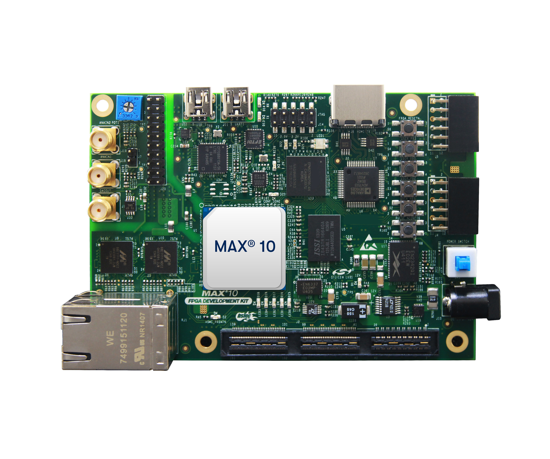
Figure 3 – MAX 10 FPGA Development Kit featuring Ethernet, HDMI, DDR3, and analog interfaces for rapid prototyping.
For development and evaluation, Altera offers the MAX 10 FPGA Development Kit with dual Gigabit Ethernet, HDMI output, DDR3 memory, and dual ADC SMA inputs. The free Quartus Prime Lite Edition supports the full design flow from RTL entry through JTAG programming.
Video Tutorial: Getting Started with MAX 10 FPGA
Related Articles on WWDParts
- 10M08SAE144C8G Datasheet & Pinout Guide – Intel MAX 10 FPGA
- 10M16SAU169C8G Specifications & Application Guide – Intel MAX 10 FPGA
- XC7A100T-1CSG324C Troubleshooting Guide – Xilinx Artix-7
6. Frequently Asked Questions (FAQ)
Q1: What is the difference between the 10M16SAU169I7G and the 10M16SAU169C8G?
The “I7” suffix indicates industrial temperature range (−40 °C to +100 °C) at speed grade 7, while the “C8” suffix indicates commercial temperature range (0 °C to +85 °C) at speed grade 8. The industrial variant is required for harsh-environment deployments such as outdoor infrastructure or factory-floor equipment.
Q2: Does the 10M16SAU169I7G require an external configuration flash?
No. The MAX 10 family integrates configuration flash on-chip, enabling instant-on operation without external EPROM or SPI flash. The device supports dual-image storage for fail-safe remote field updates.
Q3: How many ADC channels are available?
The device includes a dual 12-bit ADC block capable of up to 1 MSPS per channel. Each ADC block supports up to 9 analog input channels (directly routed to dedicated pins), providing a total of up to 18 analog inputs depending on the pin configuration.
Q4: What development tools are needed to program the 10M16SAU169I7G?
Intel Quartus Prime Lite Edition (free download) provides the complete design flow: RTL entry (Verilog/VHDL), synthesis, place-and-route, timing analysis, simulation (ModelSim-Intel Starter Edition), and device programming via JTAG or passive serial. A USB-Blaster or USB-Blaster II download cable is required for programming.
Q5: Can the MAX 10 FPGA interface with DDR3 memory?
Yes. The 10M16 device supports external DDR3, DDR2, and LPDDR2 SDRAM through a hard memory controller IP available in the Quartus Platform Designer (formerly Qsys). The U169 package supports up to a 16-bit DDR3 data bus width.
Q6: What is the maximum operating frequency of the 10M16SAU169I7G?
The four on-chip PLLs can synthesize clocks up to 500 MHz. Achievable fabric frequency depends on design complexity and timing constraints; typical registered logic in speed grade 7 can operate at 250–300 MHz for simple pipelines. The device’s fMAX for a specific design is determined by the Quartus timing analyzer after place-and-route.


