10M16SAU169I7G Datasheet, Specifications & Application Guide – Altera MAX 10 FPGA
Overview of the 10M16SAU169I7G
The 10M16SAU169I7G is a non-volatile FPGA from the Altera (Intel) MAX 10 family, manufactured on a 55 nm flash process node. It integrates 16,000 logic elements, a dual-channel 12-bit analog-to-digital converter (ADC), and internal configuration flash memory that enables instant-on operation—no external configuration device is required.
The part number decodes as follows: 10M16 = MAX 10 family with 16K logic elements, S = single power-supply mode, A = analog block (ADC) enabled, U169 = 169-ball UBGA package (7 mm × 7 mm), I = industrial temperature range (−40 °C to +100 °C), and 7 = speed grade 7.
Thanks to its integrated ADC, compact UBGA package, and low power consumption, the 10M16SAU169I7G is widely deployed in industrial automation, motor-drive controllers, sensor-fusion hubs, IoT edge gateways, and medical instrumentation. Its dual-boot capability and user flash storage make it an excellent choice for field-upgradable embedded systems.
Key Specifications & Electrical Parameters
| Parameter | Value |
|---|---|
| Manufacturer | Altera (Intel) |
| Family | MAX 10 (10M16) |
| Process Node | 55 nm Flash |
| Logic Elements (LEs) | 16,000 |
| Logic Array Blocks (LABs) | 1,000 |
| Embedded Memory (M9K) | 549 Kbit |
| User Flash Memory (UFM) | 2,876 Kbit |
| 18 × 18 Multipliers | 45 |
| PLLs | 4 |
| ADC | Dual 12-bit, 1 MSPS |
| Maximum User I/O Pins | 130 |
| Package | 169-Ball UBGA (7 mm × 7 mm, 0.5 mm pitch) |
| Core Voltage (VCC) | 1.2 V |
| I/O Voltage (VCCIO) | 1.2 V / 1.5 V / 1.8 V / 2.5 V / 3.0 V / 3.3 V |
| Operating Temperature | −40 °C to +100 °C (Industrial) |
| Speed Grade | 7 |
| Configuration | Internal flash (instant-on), dual boot |
| I/O Standards Supported | LVTTL, LVCMOS, SSTL, HSTL, LVDS, differential |
| RoHS Compliant | Yes |
Block Diagram & Internal Architecture
The MAX 10 architecture places the logic array at the center, flanked by I/O banks on all four sides. Embedded M9K memory blocks and 18×18 multiplier units are distributed throughout the fabric to support DSP-intensive applications. Four phase-locked loops (PLLs) sit at the device corners, providing flexible clock synthesis and management. The integrated dual ADC block connects to dedicated analog input pins, allowing direct sensor interfacing without external converters.

Figure 1: MAX 10 FPGA internal block diagram illustrating the logic fabric, embedded memory, DSP multiplier blocks, PLL locations, and integrated ADC.
Pinout, Package & PCB Footprint
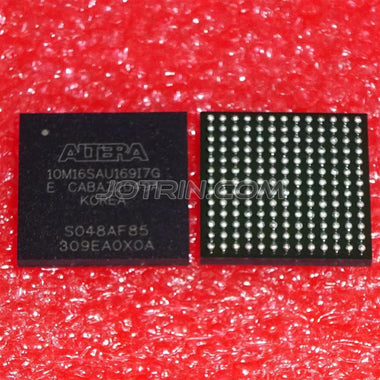
The 10M16SAU169I7G ships in a 169-ball UBGA package measuring 7 mm × 7 mm with a 0.5 mm ball pitch. The compact form factor is ideal for space-constrained designs such as wearable sensor modules and small-form-factor industrial controllers. A total of 130 user I/O pins are organized across multiple I/O banks, each independently configurable for voltage levels from 1.2 V to 3.3 V.

Figure 2: 10M16SAU169I7G in 169-ball UBGA package — 7 mm × 7 mm footprint with 0.5 mm ball pitch.
For PCB layout, Altera recommends 4-layer or 6-layer stack-ups with dedicated power and ground planes. Decoupling capacitors (100 nF ceramic) should be placed as close as possible to each VCC and VCCIO pin. The JTAG programming chain (TCK, TMS, TDI, TDO) should be routed with controlled impedance and kept away from high-speed signal traces.
Application Circuit & Reference Design
A typical application circuit for the 10M16SAU169I7G centers on a single 3.3 V supply rail that feeds an on-chip voltage regulator to generate the 1.2 V core supply. The dual ADC inputs connect directly to analog sensors (temperature, current, pressure), while digital I/O banks interface with external SDRAM, SPI flash, UART transceivers, and communication buses (I²C, SPI, LVDS). The JTAG port provides in-system programming and debug access via the Intel USB-Blaster.

Figure 3: Intel MAX 10 FPGA Development Kit — a reference platform for prototyping application circuits with the MAX 10 family.
The MAX 10 device supports dual configuration images stored in internal flash, enabling safe remote firmware updates: if the primary image fails a CRC check, the device automatically boots from the fallback image. User flash memory (UFM) can store calibration data, serial numbers, or small data logs without requiring external EEPROM.
Video: Getting Started with Intel MAX 10 FPGA
Frequently Asked Questions (FAQ)
What is the 10M16SAU169I7G and what family does it belong to?
The 10M16SAU169I7G is a non-volatile FPGA from the Altera (Intel) MAX 10 family. It contains 16,000 logic elements, an integrated dual 12-bit ADC, and built-in flash configuration memory on a 55 nm process, packaged in a 169-ball UBGA form factor rated for industrial temperatures (−40 °C to +100 °C).
Does the 10M16SAU169I7G require an external configuration memory?
No. The MAX 10 family stores its configuration bitstream in on-chip flash memory, enabling instant-on operation within milliseconds of power-up. It also supports dual configuration images for safe remote updates without any external PROM or SPI flash.
What analog capabilities does the 10M16SAU169I7G offer?
It includes a dual-channel, 12-bit successive-approximation ADC capable of 1 MSPS. This allows direct connection to temperature sensors, current shunts, and other analog signals without an external ADC chip, reducing BOM cost and PCB area.
What development tools and boards are recommended?
Intel's free Quartus Prime Lite Edition supports all MAX 10 devices. Popular development boards include the Terasic DE10-Lite, the Arrow MAX 1000, and Intel's MAX 10 FPGA Development Kit (10M50). All provide on-board USB-Blaster programming and example projects.
What are typical applications for the 10M16SAU169I7G?
Common applications include industrial motor-drive control, sensor-fusion hubs, IoT edge gateways, video pre-processing pipelines, medical instrument front-ends, and LED display controllers. Its integrated ADC and instant-on capability make it especially suited for mixed-signal embedded systems.
How does the 10M16SAU169I7G compare to the 10M16SAU169C8G?
Both devices share the same 16K LE logic fabric and 169-ball UBGA package. The key differences are temperature range (the I7G is rated for industrial −40 °C to +100 °C while the C8G covers commercial 0 °C to +85 °C) and speed grade (7 vs. 8). Choose the I7G variant for harsh-environment or extended-temperature applications.
Browse our inventory at wwdparts.com for competitive pricing and fast shipping on genuine Altera / Intel FPGA components.
Related parts you may also need: