10M16SAU169I7G Datasheet, Specifications & Application Guide – Altera MAX 10 FPGA
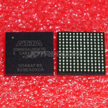
The 10M16SAU169I7G is a non-volatile FPGA from the Altera (Intel) MAX 10 family, delivering 16,000 logic elements in a compact 169-ball UBGA package. Built on a 55 nm process with integrated flash memory, dual analog-to-digital converters, and instant-on capability, this device is engineered for industrial control, IoT edge computing, and sensor-interface applications where reliable, low-power programmable logic is required.
Table of Contents
- 1. 10M16SAU169I7G Device Overview
- 2. Key Specifications & Electrical Parameters
- 3. Pinout, Package & Footprint Details
- 4. Typical Applications & Circuit Design
- 5. Design Resources & Development Kits
- 6. Frequently Asked Questions (FAQ)
1. 10M16SAU169I7G Device Overview
The 10M16SAU169I7G belongs to the MAX 10 FPGA family, the industry's first single-chip non-volatile FPGA built on TSMC's 55 nm embedded flash process. Unlike traditional FPGAs that require external configuration memory, the MAX 10 integrates configuration flash on-chip, enabling instant-on operation within milliseconds of power-up — a critical feature for automotive, industrial, and safety-critical systems.
The part number decodes as follows: 10M16 = MAX 10 family with 16K logic elements; S = single power-supply mode; A = analog block (ADC) enabled; U169 = 169-ball Ultra-Thin Fine-Pitch BGA package; I = industrial temperature range (−40°C to +100°C); 7 = speed grade 7.
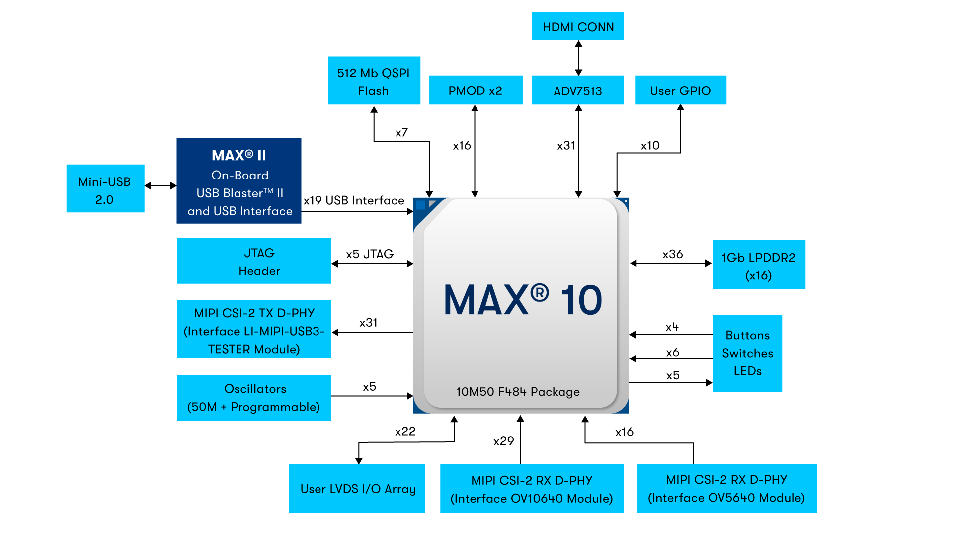
Figure 1: MAX 10 FPGA evaluation kit block diagram illustrating the internal architecture with embedded ADC, flash memory, and I/O banks.
2. Key Specifications & Electrical Parameters
| Parameter | Value |
|---|---|
| Part Number | 10M16SAU169I7G |
| Family | MAX 10 (Altera / Intel) |
| Logic Elements (LEs) | 16,000 |
| Logic Array Blocks (LABs) | 1,000 |
| Embedded Memory (M9K) | 549 Kb |
| User Flash Memory (UFM) | 2,304 Kb |
| 18×18 Multipliers | 45 |
| PLLs | 4 |
| Global Clock Networks | 20 |
| ADC | Dual 12-bit, 1 MSPS |
| Maximum User I/O | 130 |
| Package | 169-ball UBGA (11 mm × 11 mm) |
| Core Voltage (VCC) | 1.2 V |
| I/O Voltage Range | 1.0 V – 3.3 V |
| I/O Standards | LVTTL, LVCMOS, SSTL, HSTL, HSUL, LVDS |
| External Memory | DDR3, DDR2, LPDDR2 SDRAM |
| Temperature Range | −40°C to +100°C (Industrial) |
| Speed Grade | 7 |
| Process Node | 55 nm (TSMC embedded flash) |
| Configuration | Internal flash (instant-on), JTAG |
The single power-supply variant (S) simplifies board design by deriving all internal voltages from a single 3.3 V input through an integrated voltage regulator, reducing external component count and PCB area.
3. Pinout, Package & Footprint Details
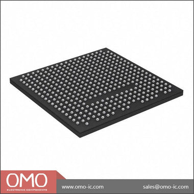
The 10M16SAU169I7G uses the U169 Ultra-Thin Fine-Pitch BGA package measuring 11 mm × 11 mm with a 0.8 mm ball pitch. This compact form factor is ideal for space-constrained designs in handheld instruments, compact sensor modules, and embedded controllers.

Figure 2: U169 UBGA-169 package mechanical drawing and ball assignment for the 10M16SAU169I7G.
Key pin categories include:
- 130 user I/O pins across multiple I/O banks supporting 3.3 V LVTTL/LVCMOS to 1.0 V differential signaling
- Dedicated analog input pins for the dual 12-bit ADC channels
- JTAG programming pins (TCK, TDI, TDO, TMS) for in-system configuration
- Power and ground pins for VCC (1.2 V core), VCCIO (per-bank), and VCCA (analog)
For complete pin assignment tables and recommended PCB land patterns, consult the MAX 10 FPGA Device Pin-Out document available from the Altera product catalog on wwdparts.com.
4. Typical Applications & Circuit Design
The 10M16SAU169I7G is widely deployed across diverse application domains:
- Industrial Automation: Motor drive control, PLC co-processors, real-time sensor fusion with on-chip ADC
- IoT Edge Nodes: Protocol bridging (SPI/I2C/UART to Ethernet), edge inference pre-processing, secure boot with bitstream encryption
- Test & Measurement: Custom data acquisition with the dual 12-bit ADC, waveform generation, high-speed digital pattern generation
- Video & Display: LED panel controllers, LVDS serializer/deserializer, video format conversion
- Communications: Baseband processing, multi-protocol bridge, custom PHY interfaces
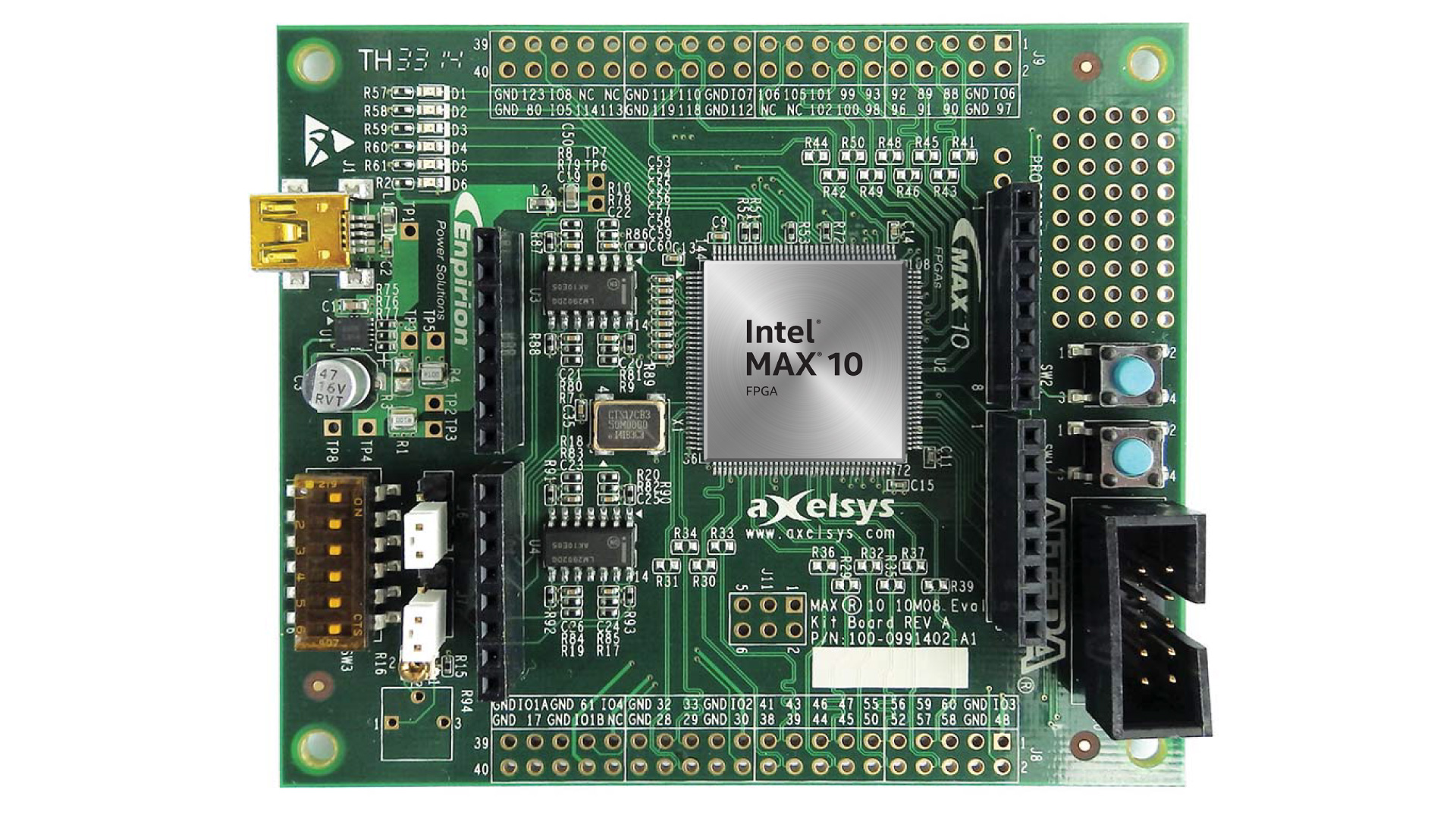
Figure 3: MAX 10 FPGA evaluation board featuring an Altera MAX 10 device with USB-Blaster, SDRAM, and Arduino-compatible expansion headers for rapid prototyping.
For power supply design, the single-supply variant requires only a 3.3 V input. The integrated regulator generates the 1.2 V core voltage internally. Add decoupling capacitors (100 nF ceramic per VCC pin, 10 µF bulk) close to the BGA for optimal signal integrity. See the MAX 10 design guides on the wwdparts blog for reference schematics.
5. Design Resources & Development Kits
Altera provides comprehensive design support for the MAX 10 family:
- Quartus Prime Lite Edition – Free FPGA design software supporting synthesis, place-and-route, timing analysis, and JTAG programming for all MAX 10 devices
- MAX 10 FPGA Development Kit – Full-featured evaluation platform with USB-Blaster II, DDR3 SDRAM, Arduino/Pmod headers, HSMC connector, and on-board power management
- Terasic DE10-Lite – Low-cost educational board featuring the MAX 10 10M50 FPGA with VGA, accelerometer, 7-segment displays, and switches — perfect for learning and prototyping
- Platform Designer (Qsys) – System integration tool for building Nios II soft-processor systems with DMA, timers, UART, and memory controllers
- ModelSim-Intel Starter Edition – Free HDL simulation environment for functional and timing verification
Video Tutorial: Getting Started with MAX 10 FPGA
Watch: Intel MAX 10 FPGA Tutorial Part 1 — covering Quartus Prime setup, pin assignment, and your first LED-blink project on a MAX 10 board.
6. Frequently Asked Questions (FAQ)
Q1: What is the difference between the 10M16SAU169I7G and the 10M16SAU169C8G?
The main differences are temperature range and speed grade. The I7G variant supports the industrial temperature range (−40°C to +100°C) with speed grade 7, while the C8G variant is rated for the commercial range (0°C to +85°C) with speed grade 8 (slower). The I7G is preferred for harsh-environment industrial and outdoor applications.
Q2: Does the 10M16SAU169I7G require external configuration flash memory?
No. The MAX 10 family integrates configuration flash memory (CFM) on-chip, enabling instant-on operation without any external EPROM or flash device. The FPGA loads its configuration from internal flash within milliseconds of power-up, significantly simplifying BOM and PCB layout.
Q3: How do I use the integrated ADC on the 10M16SAU169I7G?
The dual 12-bit ADC supports up to 1 MSPS sampling rate with up to 18 analog input channels (device and package dependent). Configure the ADC using the Altera Modular ADC IP Core in Quartus Prime. The ADC can operate in single-channel, sequencer, or temperature-sensing modes, and results are accessible through an Avalon-MM interface.
Q4: What is the maximum operating frequency of the 10M16SAU169I7G?
The maximum clock frequency depends on the design complexity and routing. Typical core logic performance reaches up to 450 MHz for register-to-register paths, while I/O data rates support up to 875 Mbps LVDS receive and 840 Mbps LVDS transmit. The 4 PLLs provide clock multiplication, division, and phase shifting for flexible clock management.
Q5: Can I run a soft processor (Nios II) on the 10M16SAU169I7G?
Yes. With 16,000 logic elements and 549 Kb of embedded SRAM, the 10M16SAU169I7G comfortably hosts a Nios II/e (economy) or Nios II/f (fast) soft processor along with peripherals such as UART, SPI, I2C, timers, and GPIO. Use Platform Designer in Quartus Prime to assemble the processor system graphically.
Q6: Where can I buy the 10M16SAU169I7G at competitive pricing?
The 10M16SAU169I7G is available from authorized distributors and specialized semiconductor suppliers. Visit wwdparts.com for competitive pricing, guaranteed-authentic stock, datasheets, and fast global shipping on Altera MAX 10 FPGAs and thousands of other electronic components.
Related Articles on wwdparts.com: