Request a Quote · 10M16SAU169I7G
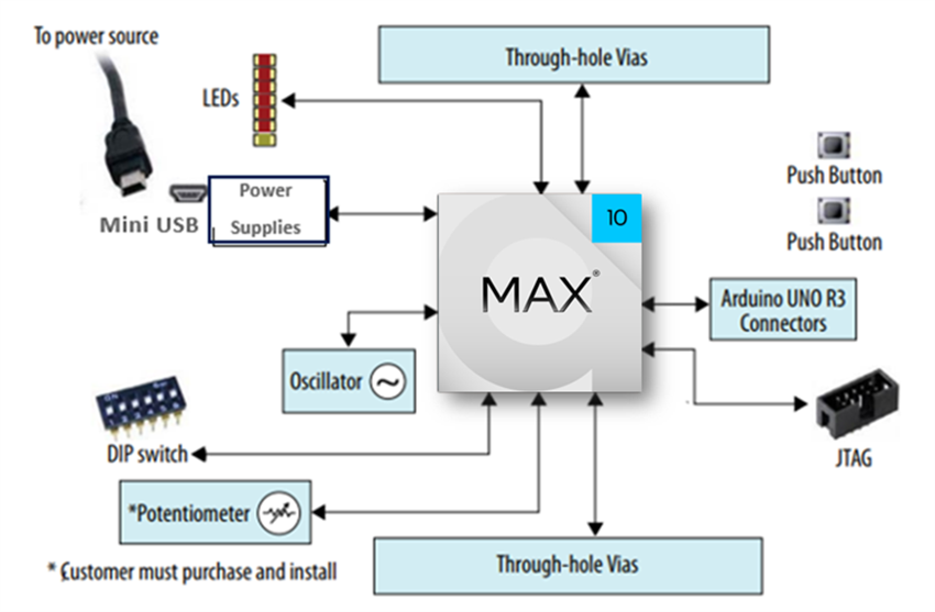
Intel MAX 10 FPGA Functional Block Diagram — Showing Logic Array, Embedded Memory, ADC Block, PLLs, and I/O Interfaces (Source: Intel/Altera)
The 10M16SAU169I7G is an Altera (now Intel) MAX 10 family FPGA featuring 16,000 logic elements, integrated dual 12-bit ADC, and non-volatile internal flash configuration memory in a compact 169-ball UBGA package. Built on 55 nm flash process technology, this device delivers instant-on capability with configuration times under 10 ms, eliminating the need for external configuration devices. Rated for industrial temperature operation (−40°C to +100°C) at speed grade 7, the 10M16SAU169I7G is engineered for demanding embedded applications in industrial control, motor drives, IoT edge gateways, sensor hubs, and medical instrumentation.
Table of Contents
1. Overview and Core Features
The MAX 10 FPGA family represents Intel’s (formerly Altera’s) single-chip, non-volatile programmable logic solution targeting cost-sensitive and space-constrained embedded designs. The 10M16SAU169I7G integrates 16,000 logic elements (LEs), 549 Kb of embedded SRAM, 2,304 Kb of user flash memory (UFM), and 45 18×18 DSP multiplier blocks, providing substantial on-chip compute and storage resources. With 4 phase-locked loops (PLLs) and support for LVDS, LVCMOS, and SSTL I/O standards, the device enables high-speed interfacing with DDR2, DDR3, LPDDR2, and SRAM external memories.
A key differentiator of the MAX 10 family is the integrated dual 12-bit analog-to-digital converter (ADC), capable of sampling up to 1 MSPS per channel. This eliminates the need for external ADC ICs in sensor acquisition, power monitoring, and temperature measurement applications. The “S” designation in the part number indicates single power-supply operation (3.0 V to 3.3 V), simplifying board-level power distribution. The “A” designator confirms the on-chip ADC is enabled, and the “I” suffix denotes industrial-grade temperature qualification (−40°C to +100°C).
The non-volatile flash-based configuration architecture enables instant-on operation in under 10 milliseconds, supports dual configuration images for remote field upgrades with automatic fallback, and provides bitstream encryption with 128-bit AES for IP security. These features make the 10M16SAU169I7G particularly well-suited for safety-critical industrial systems that require deterministic startup behavior and secure firmware management.

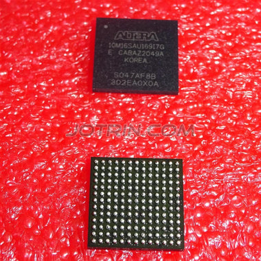
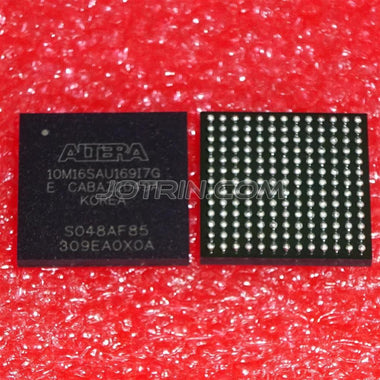
10M16SAU169I7G in 169-Ball UBGA Package — Bottom View Showing BGA Solder Ball Array (Source: FPGAkey)
2. Specifications and Parameter Table
| Parameter | Value |
|---|---|
| Manufacturer | Altera (Intel PSG) |
| Device Family | MAX 10 FPGA |
| Logic Elements (LEs) | 16,000 |
| Embedded SRAM | 549 Kb |
| User Flash Memory (UFM) | 2,304 Kb |
| DSP Multiplier Blocks (18×18) | 45 |
| Phase-Locked Loops (PLLs) | 4 |
| Maximum User I/O Pins | 130 (U169 package) |
| Analog-to-Digital Converter | Dual 12-bit ADC, up to 1 MSPS |
| External Memory Interfaces | DDR2, DDR3, LPDDR2, SRAM |
| I/O Standards Supported | LVTTL, LVCMOS, SSTL, HSTL, LVDS, LVPECL, RSDS |
| Configuration Memory | Internal Flash (non-volatile, dual image) |
| Configuration Time | < 10 ms (instant-on) |
| Bitstream Security | 128-bit AES Encryption |
| Process Technology | 55 nm Flash |
| Core Supply Voltage | 1.2 V |
| I/O Supply Voltage | 3.0 V to 3.3 V (single supply) |
| Package | 169-Ball UBGA (11 mm × 11 mm) |
| Speed Grade | 7 |
| Operating Temperature | −40°C to +100°C (Industrial) |
| RoHS Compliance | RoHS Compliant |
Looking for 10M16SAU169I7G Inventory?
Check our real-time stock levels, pricing, and volume discounts for global distribution.
Check 10M16SAU169I7G Stock3. Architecture, Pinout, and Application Circuit
The 10M16SAU169I7G internal architecture is organized around a configurable logic array of 16,000 LEs, each consisting of a 4-input look-up table (LUT), a programmable register, and carry chain logic. The embedded memory blocks are implemented as M9K blocks (each providing 9,216 bits), which can be configured as single-port RAM, dual-port RAM, ROM, or FIFO buffers. The 45 DSP blocks support 18×18 multiplication with optional accumulation, enabling efficient implementation of FIR filters, FFTs, and other signal processing algorithms without consuming general-purpose logic resources.
The integrated dual ADC subsystem features two independent 12-bit SAR analog-to-digital converters with dedicated analog input channels. The ADC block includes a temperature sensing diode for on-die thermal monitoring and supports up to 18 external analog input channels, making it possible to consolidate sensor acquisition, power rail monitoring, and environmental sensing into a single FPGA device. The ADC results are accessible through the Avalon Memory-Mapped (Avalon-MM) interface within the FPGA fabric.
In the U169 UBGA package, the device provides 130 user I/O pins organized into multiple I/O banks, each independently configurable for different voltage standards. The 4 on-chip PLLs support frequency synthesis, clock multiplication and division, and phase shifting for precise clock management. For a typical application circuit, Intel recommends a single 3.3 V supply for VCCIO banks, a 1.2 V supply for the core (VCCINT), and appropriate decoupling capacitors (100 nF + 10 µF) placed close to each power pin. The JTAG interface (TCK, TDI, TDO, TMS) is used for device programming and in-system debugging via Intel Quartus Prime software.
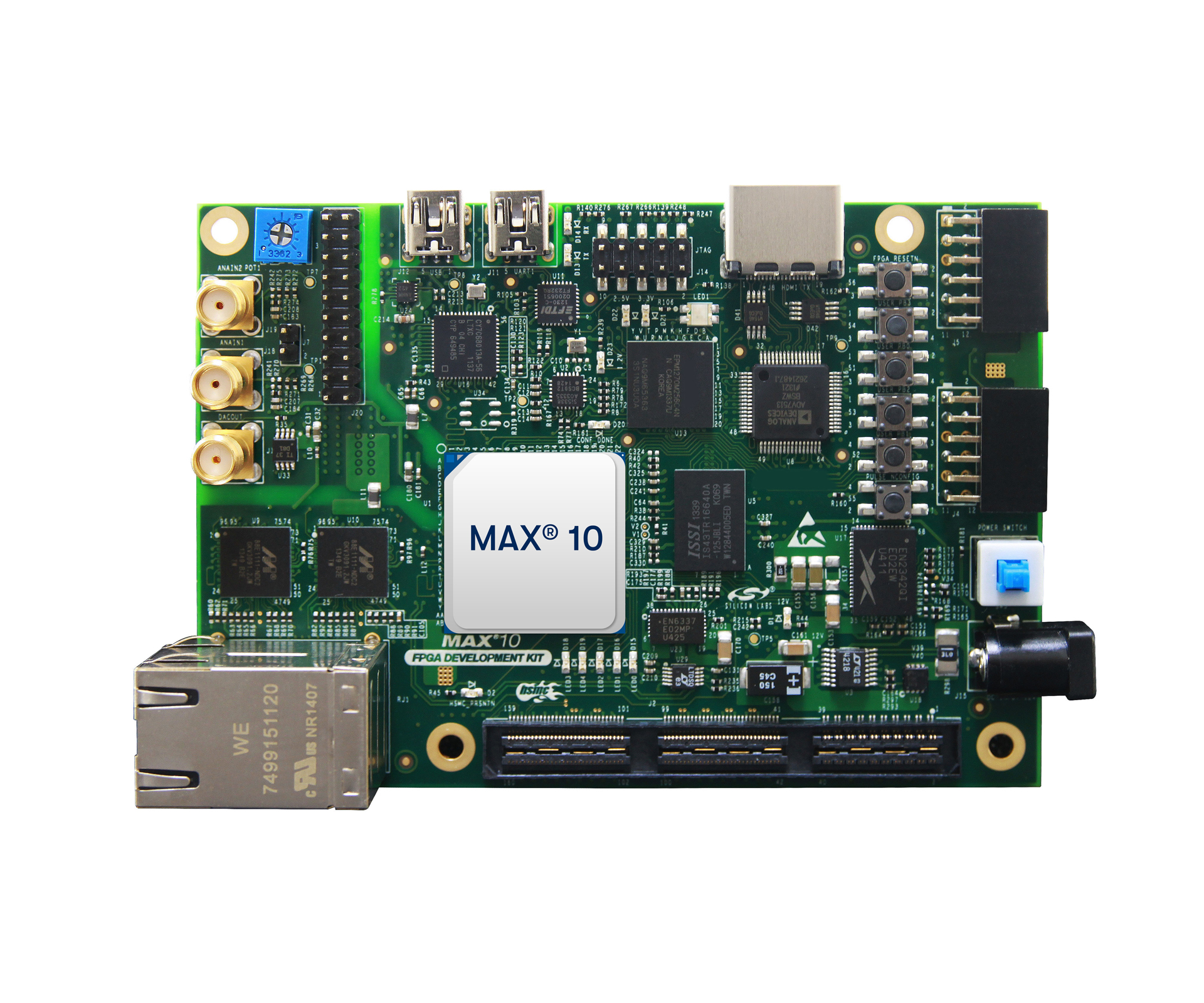
MAX 10 FPGA Development Kit — Evaluation Platform Featuring MAX 10 FPGA with DDR3 Memory, HSMC Connectors, and Onboard USB-Blaster II (Source: Altera)
4. Video: MAX 10 FPGA Development Tutorial
This video covers essential FPGA development concepts applicable to the MAX 10 family, including project setup in Intel Quartus Prime, pin assignment, design compilation, and device programming via JTAG. Whether you are implementing a simple LED blinker or a complex sensor acquisition system using the 10M16SAU169I7G’s integrated ADC, these foundational skills are critical for productive MAX 10 FPGA development.
5. Equivalents, Cross-Reference, and Lifecycle
The 10M16SAU169I7G carries an Active production status from Intel/Altera. The MAX 10 family remains a strategic product line for single-chip FPGA solutions with integrated analog capability. For designs requiring pin-compatible or functionally equivalent alternatives, consider the following options:
- 10M16SAU169C8G — Same device in the commercial temperature grade (0°C to +85°C) with speed grade 8. Suitable for cost-optimized designs without industrial temperature requirements.
- 10M25SAU169I7G — A higher-density variant in the same U169 package with 25,000 logic elements, 675 Kb embedded RAM, and 56 DSP blocks. Pin-compatible upgrade path when additional logic resources are needed.
- 10M08SAU169C8G — A lower-density option with 8,000 LEs in the same U169 package for designs with tighter cost targets and moderate logic requirements.
- Lattice MachXO3LF-6900 — A competing non-volatile FPGA from Lattice Semiconductor with 6,864 LUTs, instant-on configuration, and embedded flash. Consider as a second-source option, though pinout migration will require PCB redesign.
When migrating between MAX 10 variants, verify that the target device’s I/O count, embedded RAM capacity, and DSP block count meet your design requirements. Check 10M16SAU169I7G Inventory & Pricing at WWDParts for current lead times and global stock availability.
6. Frequently Asked Questions (FAQ)
Q1: What is the 10M16SAU169I7G, and what is it used for?
The 10M16SAU169I7G is a non-volatile FPGA from the Intel (Altera) MAX 10 family, featuring 16,000 logic elements, dual 12-bit ADC, 549 Kb embedded RAM, and 2,304 Kb user flash memory in a 169-ball UBGA package. It is widely used in industrial control, motor drives, IoT sensor hubs, video preprocessing, medical devices, and communication control planes where instant-on operation, low power, and small form factor are critical requirements.
Q2: What does the part number 10M16SAU169I7G decode to?
10M = MAX 10 family, 16 = 16K logic elements, S = single power supply, A = ADC enabled, U169 = 169-ball UBGA package, I = industrial temperature (−40°C to +100°C), 7 = speed grade 7, G = lead-free (RoHS). This coding system helps engineers quickly identify device capability, package, and operating conditions.
Q3: Does the 10M16SAU169I7G require an external configuration memory device?
No. The MAX 10 FPGA integrates on-chip flash configuration memory, which stores the FPGA bitstream internally. This eliminates the need for external serial configuration flash (such as EPCS or EPCQ devices) and enables instant-on operation with configuration complete in under 10 milliseconds after power-up. The device supports dual configuration images for safe remote field upgrades with automatic fallback to a known-good image if the primary image fails.
Q4: How do I use the integrated ADC in the 10M16SAU169I7G?
The dual 12-bit ADC is accessed through the Altera ADC IP core instantiated in Intel Quartus Prime. The ADC supports up to 18 external analog input channels (shared with digital I/O pins) plus an internal temperature sensing diode. You configure the ADC channels, sampling rate (up to 1 MSPS per ADC), and sequencing through the Quartus Platform Designer (formerly Qsys). The ADC results are read through the Avalon-MM slave interface in your FPGA logic, enabling real-time sensor data acquisition without external ADC components.
Q5: What power supply voltages are required for the 10M16SAU169I7G?
The single-supply (“S”) designation means the device operates with a simplified power architecture. The core supply (VCCINT) requires 1.2 V, while the I/O banks (VCCIO) operate at 3.0 V to 3.3 V. The analog supply for the ADC (VCCA_ADC) requires 2.5 V. Intel recommends placing 100 nF and 10 µF decoupling capacitors near each power pin, with a dedicated analog supply plane for the ADC section to minimize digital switching noise coupling into analog measurements.
Q6: What software tools are needed to program the 10M16SAU169I7G?
Intel Quartus Prime Lite Edition (free) is the primary design tool, supporting Verilog, VHDL, and schematic entry for MAX 10 devices. The toolchain includes synthesis, place-and-route, timing analysis, and the Programmer tool for JTAG-based device configuration. The Platform Designer (Qsys) is used to instantiate and connect IP cores such as the ADC controller, Nios II soft processor, and memory interfaces. Programming is performed via the onboard USB-Blaster or USB-Blaster II interface using the JTAG chain (TCK, TDI, TDO, TMS pins).