10M16SAU169I7G Datasheet, Specifications & Application Guide | Altera MAX 10 FPGA
The 10M16SAU169I7G is a non-volatile FPGA from the Altera (Intel) MAX 10 family, built on a 55 nm flash process. With 16,000 logic elements, an integrated dual 12-bit ADC, embedded SRAM, user flash memory, and instant-on capability, it delivers a highly integrated single-chip solution for industrial, IoT, and mixed-signal embedded designs. This guide covers its complete datasheet specifications, pinout, block diagram, typical application circuits, and practical design recommendations.
1. Device Overview & Part Number Decoding
The MAX 10 FPGA family eliminates external configuration devices by storing the bitstream in on-chip flash memory, enabling instant-on operation in under 10 ms. The 10M16SAU169I7G variant is optimized for single-supply, analog-enabled applications in the industrial temperature range.
Part Number Breakdown
| Segment | Value | Meaning |
|---|---|---|
| 10M16 | MAX 10, 16K LEs | Device family and logic density |
| S | Single supply | Single 3.3 V power supply for core and I/O |
| A | Analog | Integrated dual ADC enabled |
| U169 | UBGA-169 | 169-ball Ultra-Fine-Pitch BGA package |
| I | Industrial | -40 C to +100 C operating range |
| 7 | Speed grade 7 | Slowest speed grade (lowest power) |
| G | Lead-free | RoHS-compliant, green package |
2. Key Specifications & Parameters
| Parameter | Value |
|---|---|
| Logic Elements (LEs) | 16,000 |
| Logic Array Blocks (LABs) | 1,000 |
| Embedded Memory (M9K SRAM) | 549 Kb (56 M9K blocks) |
| User Flash Memory (UFM) | 2,304 Kb |
| 18 x 18 Multipliers | 45 |
| PLLs | 4 |
| Global Clock Networks | 20 |
| Max User I/O Pins (U169) | 130 |
| ADC | Dual 12-bit, up to 1 MSPS, 18 analog inputs |
| Configuration Flash | Dual-image internal flash |
| Core Voltage | 1.2 V |
| I/O Supply Voltage | 3.0 V / 3.3 V |
| I/O Standards | LVTTL, LVCMOS (1.2-3.3 V), SSTL, HSTL, LVDS |
| Package | 169-ball UBGA (11 x 11 mm, 0.8 mm pitch) |
| Operating Temperature | -40 C to +100 C (Industrial) |
| Speed Grade | 7 |
| Process Technology | 55 nm flash |
3. Block Diagram & Architecture
The MAX 10 architecture integrates logic elements, embedded M9K memory blocks, DSP multipliers, PLLs, a dual ADC block, user flash memory, and configuration flash into a single monolithic die. The block diagram below illustrates the high-level internal architecture:
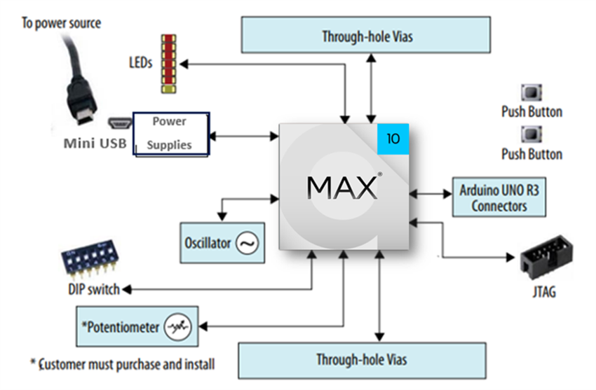
Key architectural highlights include:
- Logic Array: 16,000 LEs organized into 1,000 LABs, each containing 16 adaptive logic modules (ALMs) for efficient logic mapping.
- Embedded Memory: 56 M9K blocks providing 549 Kb of dual-port SRAM, configurable as ROM, single-port RAM, dual-port RAM, or FIFO buffers.
- DSP Blocks: 45 embedded 18 x 18 multipliers supporting multiply-accumulate operations for digital signal processing.
- Integrated ADC: Dual 12-bit successive-approximation ADC with up to 18 external analog inputs and an internal temperature sensor.
- Clock Management: 4 PLLs with up to 20 global clock networks for flexible clock generation and distribution.
4. Pinout & Package Information
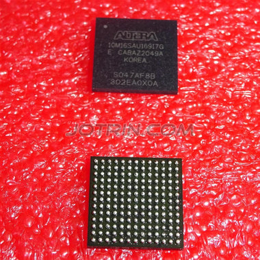
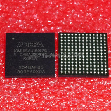
The 10M16SAU169I7G is packaged in a 169-ball UBGA measuring 11 x 11 mm with a 0.8 mm ball pitch. It provides up to 130 user I/O pins across multiple I/O banks supporting a wide range of voltage standards from 1.2 V to 3.3 V.

Pin assignment considerations for the U169 package:
- Power Pins: Dedicated VCC (1.2 V core), VCCIO (per-bank, 1.2-3.3 V), and GND pins distributed across the ball array for low-impedance power delivery.
- Configuration Pins: JTAG (TCK, TDI, TDO, TMS) for programming and debug; nCONFIG, nSTATUS, CONF_DONE for configuration control.
- ADC Inputs: Dedicated analog input pins (ANAIN1-ANAIN18) shared with digital I/O on selected pins; REFGND and VREF for ADC reference.
- Clock Inputs: Dedicated CLK pins for each PLL; global clock inputs distributed to all quadrants.
5. Application Circuits & Design Guide
The 10M16SAU169I7G is widely used in industrial control, motor drives, sensor hubs, IoT edge gateways, video pre-processing, and medical instrumentation. Its integrated ADC and instant-on capability make it ideal for mixed-signal embedded systems that need to be operational immediately at power-up.

Typical Application: Industrial Sensor Hub
A common design pattern uses the 10M16SAU169I7G as a sensor fusion hub. The integrated ADC samples analog sensors (temperature, pressure, current) while the FPGA fabric implements digital filtering, protocol conversion (SPI/I2C to Ethernet or UART), and local decision logic. The dual configuration flash enables safe over-the-air firmware updates in deployed field equipment.
Power Supply Recommendations
- VCC (1.2 V core): Use a low-noise LDO or DC-DC converter with output capacitance per the Power Management section of the MAX 10 datasheet.
- VCCIO (3.3 V): In single-supply mode, all I/O banks are powered at 3.3 V. Decouple each VCCIO pin with 100 nF ceramic capacitors placed as close to the BGA pads as possible.
- VCCA_ADC: Provide a clean, filtered 2.5 V supply for the ADC analog circuitry to minimize noise coupling.
Design Resources
Intel Quartus Prime Lite Edition (free) fully supports the 10M16SAU169I7G. Popular development boards include the Terasic DE10-Lite and Arrow MAX1000, both of which feature MAX 10 FPGAs with USB-Blaster programming, onboard memory, and expansion headers for rapid prototyping.
Video Tutorial
Watch this getting-started tutorial for Intel MAX 10 FPGA development with Quartus Prime:
Related Parts on WWDParts
- 10M16SAU169C8G Datasheet & Specs - Intel MAX 10 FPGA (Commercial Grade)
- 10M08SAE144C8G Datasheet & Pinout - Intel MAX 10 FPGA (8K LEs, 144-EQFP)
- 10M16SAU169I7G Previous Edition - Altera MAX 10 FPGA Guide
6. Frequently Asked Questions
Q1: What is the 10M16SAU169I7G?
The 10M16SAU169I7G is a non-volatile FPGA from the Intel (Altera) MAX 10 family. It integrates 16,000 logic elements, a dual 12-bit ADC, 549 Kb embedded SRAM, 2,304 Kb user flash memory, and 45 DSP multipliers in a compact 169-ball UBGA package rated for the industrial temperature range (-40 C to +100 C).
Q2: What package does the 10M16SAU169I7G use?
It is housed in a 169-ball Ultra-Fine-Pitch BGA (UBGA) package measuring approximately 11 x 11 mm with a 0.8 mm ball pitch, making it well-suited for space-constrained embedded designs.
Q3: Does the 10M16SAU169I7G have an integrated ADC?
Yes. The device includes a dual-channel 12-bit successive-approximation ADC capable of up to 1 MSPS, with up to 18 analog input channels. This eliminates the need for an external ADC in many mixed-signal applications.
Q4: What is the operating temperature range?
The 10M16SAU169I7G is rated for the industrial temperature range: -40 C to +100 C junction temperature, suitable for harsh-environment deployments in factory automation, outdoor IoT gateways, and automotive-adjacent systems.
Q5: What software is needed to program the 10M16SAU169I7G?
Intel Quartus Prime Lite Edition (free) fully supports all MAX 10 devices including the 10M16SAU169I7G. It provides synthesis, place-and-route, timing analysis, and JTAG programming via USB-Blaster.
Q6: Can the 10M16SAU169I7G be used for remote system updates?
Yes. MAX 10 FPGAs feature dual configuration flash memory, enabling a factory-safe image alongside an application image. This allows secure remote firmware updates with automatic fallback to the factory image if the update fails.