
10M16SAU169I7G Datasheet, Specifications & Application Guide – Altera MAX 10 FPGA
1. Overview of the 10M16SAU169I7G
The 10M16SAU169I7G is a non-volatile FPGA from the Altera (Intel) MAX 10 family, built on a 55 nm process node. Featuring 16,000 logic elements (LEs), an integrated dual 12-bit analog-to-digital converter (ADC), and internal flash configuration memory, the MAX 10 family eliminates the need for an external configuration device—enabling instant-on operation ideal for industrial, automotive-adjacent, and IoT edge applications.
The part number decodes as follows: 10M16 = MAX 10 with 16 K LEs, S = single power-supply, A = analog (ADC enabled), U169 = 169-ball UBGA package, I = industrial temperature (−40 °C to +100 °C), and 7 = speed grade 7. If you are sourcing this component, browse our Altera inventory at wwdparts.com for competitive pricing and fast delivery.
2. Key Specifications & Parameters
| Parameter | Value |
|---|---|
| Part Number | 10M16SAU169I7G |
| Family | Intel / Altera MAX 10 |
| Logic Elements (LEs) | 16,000 |
| Logic Array Blocks (LABs) | 1,000 |
| Embedded Memory (M9K RAM) | 549 Kb |
| User Flash Memory (UFM) | 2,304 Kb |
| 18 × 18 Multipliers | 45 |
| PLLs | 4 |
| Analog-to-Digital Converter | Dual 12-bit, 1 MSPS SAR ADC |
| Maximum User I/O (U169) | 130 |
| LVDS Pairs (max) | 22 |
| Package | 169-UBGA (11 × 11 mm, 0.8 mm pitch) |
| Core Voltage | 1.2 V |
| I/O Voltage | 3.0 V / 3.3 V (supports 1.2 V–3.3 V standards) |
| Operating Temperature | −40 °C to +100 °C (Industrial) |
| Speed Grade | 7 |
| Process Technology | 55 nm |
| Configuration | Internal flash – instant-on, non-volatile |
| External Memory Interfaces | DDR3, DDR2, LPDDR2 SDRAM |
| RoHS Compliant | Yes (Pb-free / Green) |
3. Block Diagram & Architecture
The MAX 10 architecture integrates logic elements, embedded memory blocks, DSP multipliers, PLLs, a dual ADC, and user flash memory into a single monolithic die. Below is the functional block diagram of the MAX 10 FPGA platform:

Key architectural highlights include the integrated dual 12-bit ADC for mixed-signal designs, four fabric PLLs supporting clock management up to 500 MHz, and instant-on configuration from internal flash that eliminates boot latency. For a deeper look at MAX 10 architecture, visit the wwdparts semiconductor blog.
4. Pinout & Package Information
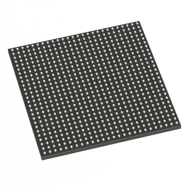
The 10M16SAU169I7G is housed in a 169-ball UBGA (Ultra-thin Ball Grid Array) package measuring 11 × 11 mm with a 0.8 mm ball pitch. This compact form factor is suitable for space-constrained embedded designs. The device provides up to 130 user I/O pins organized across multiple I/O banks supporting a wide range of voltage standards from 1.2 V LVCMOS to 3.3 V LVTTL, SSTL, and HSTL.
For differential signaling, the package supports up to 22 LVDS pairs, making it suitable for high-speed serial interfaces. The single power-supply variant (S designation) simplifies board design by requiring only a 3.3 V input supply, with the 1.2 V core voltage generated by an integrated regulator.
5. Applications & Development Kits
The 10M16SAU169I7G is widely used in industrial control systems, motor drives, sensor hubs, IoT edge gateways, video surveillance pre-processing, and medical instrumentation. Its integrated ADC and instant-on capability make it particularly attractive for mixed-signal embedded designs where a separate microcontroller-plus-FPGA topology would be too costly or space-consuming.

Altera offers the MAX 10 FPGA Development Kit and the popular Terasic DE10-Lite board for rapid prototyping. These kits include on-board USB-Blaster programming, SDRAM, VGA output, Arduino-compatible expansion headers, and accelerometer sensors. The free Quartus Prime Lite Edition provides synthesis, place-and-route, and JTAG programming support for all MAX 10 devices. Explore related FPGA components in our Intel FPGA collection at wwdparts.com.
Video: MAX 10 FPGA Development Kit Overview
6. Frequently Asked Questions (FAQ)
What is the 10M16SAU169I7G?
The 10M16SAU169I7G is an Intel/Altera MAX 10 family FPGA with 16,000 logic elements, a dual 12-bit ADC, 549 Kb embedded RAM, 2,304 Kb user flash memory, and 45 DSP multipliers. It comes in a 169-UBGA package and operates across the industrial temperature range of −40 °C to +100 °C.
Does the 10M16SAU169I7G require an external configuration device?
No. The MAX 10 FPGA stores its configuration in internal flash memory, providing non-volatile instant-on operation without needing an external EPROM, serial flash, or configuration controller. This significantly simplifies BOM and PCB design.
What development tools support the 10M16SAU169I7G?
The device is supported by Intel Quartus Prime Lite Edition (free), which provides synthesis, place-and-route, timing analysis, and JTAG/SPI programming. It also supports the Nios II soft-core processor for embedded software development and ModelSim for simulation.
What is the difference between the 10M16SAU169I7G and 10M16SAU169C8G?
Both share the same 16K LE die and 169-UBGA package. The I7G variant features industrial temperature range (−40 °C to +100 °C) with speed grade 7, while the C8G variant is rated for commercial temperature (0 °C to +85 °C) with speed grade 8 (faster). Choose I7G for harsh-environment or extended-temperature applications.
What memory interfaces does the 10M16SAU169I7G support?
The MAX 10 FPGA supports external DDR3, DDR2, and LPDDR2 SDRAM interfaces through its hard memory controller IP. Internally, it provides 549 Kb of M9K embedded SRAM blocks and 2,304 Kb of user flash memory for data storage.
Where can I buy the 10M16SAU169I7G?
The 10M16SAU169I7G is available from authorized distributors and semiconductor marketplaces. You can purchase it at wwdparts.com with competitive pricing, verified inventory, and worldwide shipping.


