
10M16SAU169I7G: Altera MAX 10 FPGA - Datasheet, Pinout, Specifications & Applications
The 10M16SAU169I7G is a high-performance, non-volatile FPGA from Altera's (now Intel) MAX 10 family. Built on a 55nm flash process, this device delivers 16,000 logic elements in a compact 169-pin UBGA package, making it ideal for industrial control, motor drive, and cost-sensitive embedded designs. In this comprehensive guide, we cover datasheet specifications, pinout details, block diagrams, application circuits, and frequently asked questions about the 10M16SAU169I7G.
Table of Contents
- 1. 10M16SAU169I7G Overview
- 2. Key Specifications & Parameters
- 3. Block Diagram
- 4. Pinout & Package Information
- 5. Application Circuits & Design Examples
- 6. Frequently Asked Questions (FAQ)
1. 10M16SAU169I7G Overview
The 10M16SAU169I7G belongs to the Intel MAX 10 FPGA family, which integrates features traditionally found in separate devices — including an analog-to-digital converter (ADC), dual configuration flash memory, and user flash memory — all within a single, low-cost FPGA. The "I7G" speed and temperature grade suffix indicates an industrial temperature range of -40°C to +100°C, making it suitable for harsh operating environments.
Unlike traditional FPGAs that require external configuration memory, the MAX 10 features internal configuration storage, enabling instant-on functionality and reducing board area by eliminating external flash components. The device supports dual boot images and remote system updates, providing robust in-field upgradeability.
2. Key Specifications & Parameters
| Parameter | Value |
|---|---|
| Part Number | 10M16SAU169I7G |
| Device Family | MAX 10 (Intel / Altera) |
| Logic Elements (LEs) | 16,000 |
| Logic Array Blocks (LABs) | 1,000 |
| Embedded Memory | 549 Kb (M9K Blocks) |
| User Flash Memory | Up to 736 Kb (UFM) |
| 18×18 Multipliers | 45 |
| PLLs | 4 |
| Maximum User I/O | 130 (U169 package) |
| LVDS Pairs | Up to 22 |
| ADC (Analog-to-Digital) | Yes (12-bit, up to 1 MSPS) |
| Package Type | 169-UBGA (11 mm × 11 mm) |
| Process Technology | 55 nm Flash |
| Core Voltage | 1.2 V |
| I/O Voltage | 3.0 V / 3.3 V (LVTTL/LVCMOS) |
| Operating Temperature | -40°C to +100°C (Industrial) |
| Speed Grade | 7 (Slowest) |
| Configuration | Internal dual-boot flash |
| External Memory Interface | DDR2, DDR3, LPDDR2, SRAM |
| I/O Standards | LVTTL, LVCMOS, SSTL, HSTL, HSUL, PCI |
| Mounting | SMD / SMT (BGA) |
| FPGA Bitstream Security | Yes (AES-128 encryption) |
| RoHS Compliant | Yes |
3. Block Diagram
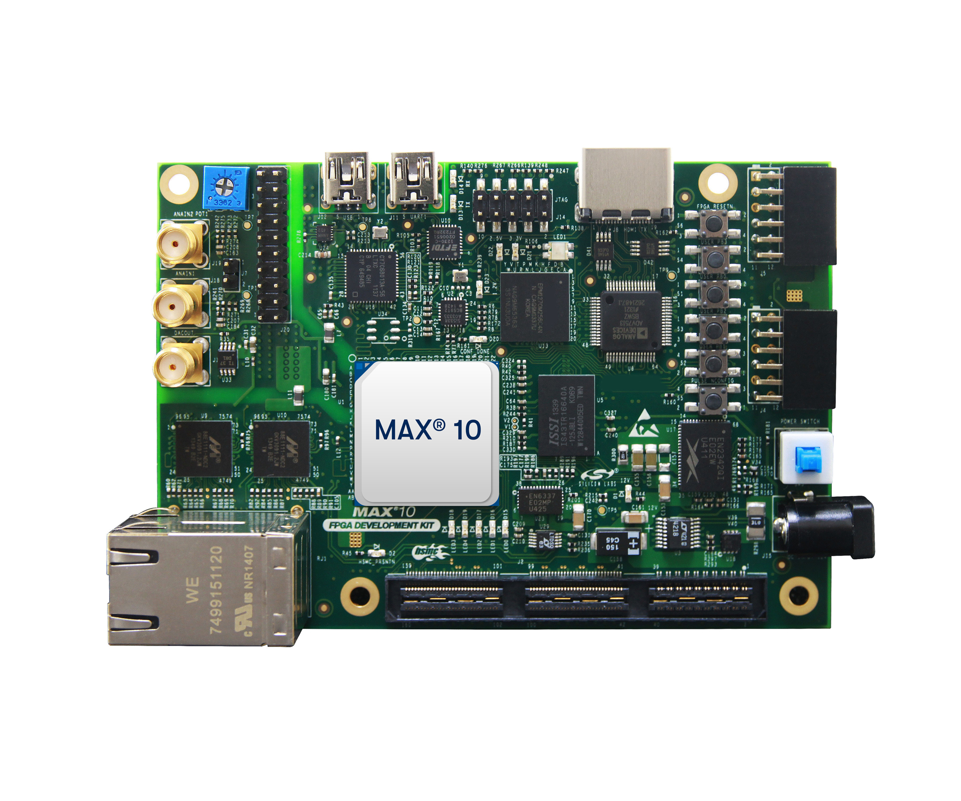
The following block diagram illustrates the MAX 10 FPGA Development Kit architecture, showcasing how the 10M16SAU169I7G interfaces with external peripherals including DDR3 memory, ADC inputs, JTAG configuration, and user I/O headers.

The MAX 10 architecture integrates logic array blocks (LABs), embedded memory (M9K blocks), 18×18 multiplier DSP blocks, and up to 4 PLLs for clock management. The built-in ADC block provides analog input capability without requiring external components.
4. Pinout & Package Information
The 10M16SAU169I7G is housed in a 169-ball UBGA (Ultra-Thin Ball Grid Array) package measuring 11 mm × 11 mm with a 0.8 mm ball pitch. This compact footprint is ideal for space-constrained designs in industrial, IoT, and portable instrumentation applications.

The U169 package provides 130 user I/O pins organized across multiple I/O banks, supporting a wide range of voltage standards from 1.0 V to 3.3 V. Pin assignments follow Altera's standard MAX 10 pinout conventions, and designers can use the Intel Quartus Prime Pin Planner for detailed pin mapping and bank assignments.
5. Application Circuits & Design Examples
The 10M16SAU169I7G is well-suited for a variety of embedded and industrial applications. The image below shows the MAX 10 FPGA Development Kit, which serves as a reference design platform for prototyping applications with this device family.
Common application areas for the 10M16SAU169I7G include:
- Industrial Motor Control: Leveraging the built-in ADC for sensor feedback and logic elements for PWM generation
- Video & Image Processing: Using embedded multipliers for real-time filtering and transformation pipelines
- Sensor Hubs & IoT Gateways: Integrating multiple sensor inputs via the ADC and programmable I/O
- Protocol Bridging: Converting between SPI, I2C, UART, and other communication interfaces
- Power Supply Monitoring: Utilizing the ADC for voltage and current measurement with instant-on boot capability
Video Tutorial: Getting Started with MAX 10 FPGA
6. Frequently Asked Questions (FAQ)
Q1: What is the difference between 10M16SAU169I7G and 10M16SAU169C8G?
The primary differences are temperature range and speed grade. The 10M16SAU169I7G operates at industrial temperature (-40°C to +100°C) with speed grade 7, while the 10M16SAU169C8G is rated for commercial temperature (0°C to +85°C) with speed grade 8. The "I" suffix denotes industrial, and "C" denotes commercial.
Q2: Does the 10M16SAU169I7G require external configuration memory?
No. The MAX 10 FPGA family features internal dual configuration flash memory, eliminating the need for external EEPROM or flash chips. This enables instant-on operation and reduces BOM cost and board area. The device supports dual boot images for safe remote updates.
Q3: What software is needed to program the 10M16SAU169I7G?
You need Intel Quartus Prime Lite Edition (free) or Quartus Prime Standard Edition. The Lite edition fully supports all MAX 10 devices. Programming is done via JTAG using an Intel USB-Blaster or compatible programmer. The Quartus Prime software includes synthesis, place-and-route, timing analysis, and the Pin Planner tool.
Q4: Can the built-in ADC be used for analog signal acquisition?
Yes. The MAX 10 FPGA integrates a 12-bit SAR ADC capable of up to 1 MSPS (mega-samples per second). It supports up to 18 analog input channels (depending on the package variant) and includes an internal temperature sensor. The ADC is configured through the Quartus Prime IP Catalog using the Altera Modular ADC IP core.
Q5: What is the maximum operating frequency of the 10M16SAU169I7G?
The maximum operating frequency depends on your specific design and resource utilization. Typical MAX 10 devices achieve up to 300 MHz for internal register-to-register paths. The speed grade 7 indicates this is the slowest speed grade in the MAX 10 lineup (grades 6, 7, 8), so timing-critical designs should carefully review the device datasheet timing parameters.
Q6: Is the 10M16SAU169I7G suitable for automotive or high-reliability applications?
The 10M16SAU169I7G is rated for industrial temperature (-40°C to +100°C), which covers many harsh-environment use cases. However, for automotive-grade (AEC-Q100) or military-grade applications, you should consult Intel/Altera for specific qualified part numbers. The "G" suffix in the part number indicates lead-free (RoHS-compliant) packaging.


