
10M16SAU169I7G: Intel (Altera) MAX 10 FPGA – Complete Technical Guide
The 10M16SAU169I7G is a highly integrated, non-volatile FPGA from the Intel (formerly Altera) MAX 10 family. Built on a 55nm flash process, this device delivers 16,000 logic elements, integrated dual ADCs, user flash memory, and internal configuration storage in a compact UBGA-169 package. Its industrial temperature rating (-40°C to +100°C) and single-chip architecture make it a compelling choice for embedded control, sensor processing, and board management applications where reliability, low power, and small form factor are paramount.
In this guide, we provide an in-depth look at the 10M16SAU169I7G specifications, architecture, pinout, target applications, and frequently asked questions to help you evaluate this FPGA for your next design. For more semiconductor articles, visit the WWD Parts Blog.
Table of Contents
- Overview and Key Features
- Detailed Specifications
- Architecture and Block Diagram
- Pinout and Package Information
- Applications and Development
- Frequently Asked Questions
1. Overview and Key Features
The Intel MAX 10 FPGA family represents a significant step forward in non-volatile FPGA design. Unlike SRAM-based FPGAs that require external configuration memory and a boot sequence, the 10M16SAU169I7G stores its configuration internally and is operational almost immediately after power-up. This instant-on capability is essential in safety-critical systems, industrial controllers, and any application where boot latency is unacceptable.
Key features that set the 10M16SAU169I7G apart include:
- 16,000 Logic Elements (LEs) organized in approximately 1,000 Logic Array Blocks (LABs), providing substantial programmable logic density for mid-range designs.
- Integrated Dual 12-bit ADCs that eliminate the need for external analog-to-digital converters, reducing BOM cost and board area.
- 549 Kb of Embedded Memory (562,176 bits) configurable as RAM, ROM, FIFO, or shift registers.
- User Flash Memory (up to 736 Kb) for storing application data, calibration constants, or firmware parameters without an external EEPROM or flash device.
- Internal Configuration Storage supporting dual boot images for safe remote firmware updates.
- 18x18 Embedded Multipliers for efficient DSP operations including filtering, signal conditioning, and mathematical computations.
- 4 PLLs providing flexible clock management with frequency synthesis and phase alignment.
- Industrial Temperature Range (-40°C to +100°C) for reliable operation in demanding environments.
Whether you are designing a sensor fusion platform, an industrial motor controller, or a compact data acquisition system, the 10M16SAU169I7G delivers the logic density, analog integration, and robustness to get the job done in a single chip. Browse our full semiconductor inventory for availability and pricing.
2. Detailed Specifications
The following table summarizes the key electrical, physical, and functional specifications of the 10M16SAU169I7G.
| Parameter | Value |
|---|---|
| Part Number | 10M16SAU169I7G |
| Family | Intel (Altera) MAX 10 FPGA |
| Logic Elements (LEs) | 16,000 |
| Logic Array Blocks (LABs) | ~1,000 |
| Embedded Memory | 549 Kb (562,176 bits) |
| User Flash Memory | Up to 736 Kb |
| 18x18 Multipliers (DSP) | Yes (embedded multiplier blocks) |
| PLLs | 4 |
| Integrated ADC | Dual 12-bit SAR ADC (up to 1 MSPS) |
| Internal Configuration | Yes (dual-image support, no external config device) |
| Max User I/O (U169 package) | 130 |
| Max User I/O (across packages) | 320 |
| Max LVDS Pairs | 22 |
| Package | UBGA-169 (Ultra-thin Ball Grid Array) |
| Core Supply Voltage | 1.2V |
| I/O Supply Voltage | 3.3V |
| Temperature Range | -40°C to +100°C (Industrial, I7G suffix) |
| Speed Grade | 7 (lowest speed, lowest power) |
| Process Technology | 55nm Flash (TSMC) |
| Supported I/O Standards | LVTTL, LVCMOS, PCI, SSTL, HSTL, LVDS, and more |
| External Memory Interfaces | DDR2, DDR3, LPDDR2, SRAM |
| RoHS Compliant | Yes |
3. Architecture and Block Diagram
The MAX 10 architecture combines a traditional FPGA logic fabric with several hard IP blocks that are typically found only on SoC-class devices. Understanding the internal architecture is essential for optimizing your design and taking full advantage of the 10M16SAU169I7G's capabilities.

Logic Array Blocks (LABs): The 16,000 logic elements are grouped into approximately 1,000 LABs. Each LAB contains 16 adaptive logic modules (ALMs) or LEs that can implement combinational and sequential logic. The interconnect architecture uses a combination of local, row, and column routing to provide high utilization and predictable timing.
Embedded Memory: The 549 Kb of embedded memory is distributed across M9K memory blocks. Each M9K block provides 9,216 bits of dual-port memory that can be configured as simple dual-port RAM, true dual-port RAM, single-port RAM, ROM, or FIFO buffers. These blocks support byte-enable, parity, and ECC features for data integrity.
DSP Blocks: The 18x18 embedded multipliers enable efficient multiply-accumulate (MAC) operations essential for digital filtering, PID control loops, and signal processing pipelines. These hard multipliers are significantly faster and more power-efficient than equivalent soft-logic implementations.
Dual ADC: The integrated analog-to-digital converters feature 12-bit resolution with up to 1 MSPS sample rate. They include a built-in temperature sensor, support for external analog channels, and a prescaler for higher-voltage inputs. The ADC results are accessible through a simple Avalon memory-mapped interface in the FPGA fabric.
Clock Management: Four PLLs provide clock synthesis, multiplication, division, and phase shifting. Each PLL includes up to five output counters, enabling a single reference clock to generate multiple system clocks with precise frequency and phase relationships.
4. Pinout and Package Information
The 10M16SAU169I7G is housed in a UBGA-169 (Ultra-thin Ball Grid Array) package with 169 balls arranged in a 13x13 grid. This compact package measures approximately 11 mm x 11 mm, making it ideal for space-constrained designs.

Key pinout considerations for the UBGA-169 package:
- User I/O Pins: Up to 130 general-purpose I/O pins organized across multiple I/O banks. Each bank can support independent voltage levels (1.2V, 1.5V, 1.8V, 2.5V, or 3.3V).
- Power Pins: Dedicated VCC (1.2V core), VCCIO (per I/O bank), VCCA (analog PLL supply), and GND balls are distributed throughout the package for low-inductance power delivery.
- Configuration Pins: JTAG interface pins (TCK, TDI, TDO, TMS) for programming and debug. Since configuration is internal, there are no dedicated pins for external flash.
- ADC Pins: Dedicated analog input pins for the dual ADC channels, plus analog power and reference pins (VREFP, VREFN, ANAIN).
- LVDS Pairs: Up to 22 differential LVDS pairs for high-speed serial interfaces, useful for display connections, sensor links, or inter-board communication.
When designing your PCB, refer to the Intel MAX 10 FPGA Pin Connection Guidelines for proper decoupling, power sequencing, and unused pin handling. A minimum of 100 nF decoupling capacitors should be placed on every VCCIO and VCC pin, located as close to the BGA balls as possible.
5. Applications and Development
The combination of integrated ADCs, flash storage, instant-on capability, and industrial-grade temperature rating makes the 10M16SAU169I7G well suited for a broad range of applications.
Target Applications
- Industrial Automation and Motor Control: The integrated ADCs handle sensor feedback while the FPGA logic implements PID loops, PWM generation, and communication protocols (EtherCAT, PROFINET, Modbus) in a single chip.
- Data Acquisition Systems: Combine the on-chip ADCs with FPGA-based digital filtering and DDR3 memory interfaces to build compact, high-channel-count DAQ systems.
- Board Management Controllers: Use the instant-on feature, user flash, and ADC for power sequencing, voltage monitoring, and system health management in servers and networking equipment.
- Automotive Sensor Hubs: The industrial temperature range and non-volatile configuration make this FPGA suitable for aggregating LIDAR, radar, and camera data in ADAS subsystems.
- Portable and Battery-Powered Instruments: Speed grade 7 offers the lowest power consumption in the MAX 10 lineup, extending battery life in handheld test equipment and field instruments.
- Communication Protocol Bridges: Implement SPI-to-Ethernet, UART-to-USB, or custom protocol conversion with on-chip memory and flexible I/O standards.
Development Ecosystem
Intel provides comprehensive tool support for the MAX 10 family. The Intel Quartus Prime Lite Edition is available as a free download and includes full support for the 10M16SAU169I7G. Key development resources include:
- Quartus Prime Lite: Free synthesis, place-and-route, timing analysis, and programming tools.
- Platform Designer (Qsys): System integration tool for connecting soft-core processors (Nios II), memory controllers, ADC interfaces, and custom peripherals.
- ModelSim Intel FPGA Edition: Free functional simulation for design verification.
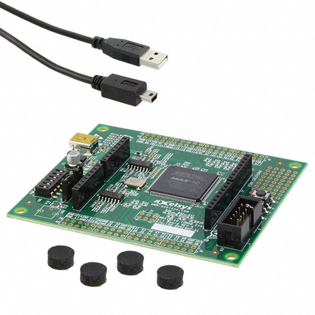
- MAX 10 FPGA Evaluation Kits: Low-cost development boards for rapid prototyping and evaluation.
- Intel FPGA IP Library: Pre-verified IP cores for DDR3 controllers, PCI Express, Nios II processors, and signal processing functions.
The following video provides an introduction to the Intel MAX 10 FPGA platform and its capabilities:
To learn more about our company and sourcing capabilities, visit the About Us page.
6. Frequently Asked Questions
What is the 10M16SAU169I7G?
The 10M16SAU169I7G is an Intel (formerly Altera) MAX 10 FPGA featuring 16,000 logic elements, dual integrated 12-bit ADCs, internal configuration storage, and user flash memory. It is housed in a compact UBGA-169 package and rated for the industrial temperature range of -40°C to +100°C. The MAX 10 family is built on a 55nm flash process that enables non-volatile, instant-on operation without external configuration devices.
What is the operating temperature range of the 10M16SAU169I7G?
The 10M16SAU169I7G operates over the industrial temperature range of -40°C to +100°C, as indicated by the I7G suffix in the part number. The "I" denotes industrial grade, the "7" indicates speed grade 7, and the "G" signifies lead-free (RoHS-compliant) packaging. This extended temperature range makes it suitable for harsh-environment applications including factory automation, outdoor communications equipment, and automotive subsystems.
Does the 10M16SAU169I7G require an external configuration device?
No. One of the defining features of the MAX 10 FPGA family is internal configuration flash memory. The 10M16SAU169I7G stores its configuration bitstream on-chip, eliminating the need for external serial configuration devices (such as EEPROM or SPI flash). This reduces BOM cost, saves board space, and simplifies the supply chain. The device also supports dual configuration images, enabling safe remote firmware updates with automatic fallback to a known-good image.
What ADC capabilities does the 10M16SAU169I7G have?
The 10M16SAU169I7G integrates dual 12-bit successive-approximation (SAR) ADCs with up to 1 MSPS throughput per channel. These on-chip ADCs support both dedicated analog input pins and an internal temperature sensing diode. They are useful for monitoring power supply voltages, reading external sensor signals, and performing on-die thermal management. The ADC block is controlled through a simple register interface mapped into the FPGA fabric via an Avalon memory-mapped bus.
What package is the 10M16SAU169I7G available in?
The 10M16SAU169I7G is packaged in a UBGA-169 (Ultra-thin Ball Grid Array) with 169 balls in a 13x13 array. The package provides up to 130 user I/O pins across multiple I/O banks. Its compact footprint (approximately 11 mm x 11 mm) and low profile make it well suited for space-constrained embedded systems, portable instruments, and high-density board designs where vertical clearance is limited.
What speed grade is the 10M16SAU169I7G?
The 10M16SAU169I7G has a speed grade of 7, which is the slowest (and lowest-power) speed grade offered in the MAX 10 family. While speed grade 6 devices achieve higher maximum clock frequencies, speed grade 7 devices provide lower static and dynamic power consumption. For many embedded control, sensor processing, and protocol bridging applications, speed grade 7 delivers more than adequate performance while extending battery life and simplifying thermal management. If your design requires the highest possible performance from the MAX 10 16K LE device, consider the speed grade 6 variant (10M16SAU169C8G).
The 10M16SAU169I7G is available through WWD Parts. We supply original, factory-sealed Intel FPGAs with full traceability and competitive pricing. Search our inventory or contact us for a quote today.


