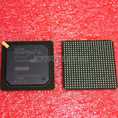
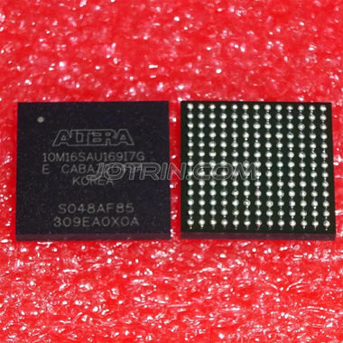
10M16SAU169I7G Datasheet, Specifications & Application Guide – Altera MAX 10 FPGA
The 10M16SAU169I7G is a non-volatile FPGA from the Intel (Altera) MAX 10 family, built on a 55 nm process node. Featuring 16,000 logic elements, an integrated dual 12-bit ADC, and internal flash configuration memory, this device delivers instant-on capability in a compact 169-ball UBGA package. It is designed for industrial-grade applications operating across the full −40 °C to +100 °C temperature range. Whether you are building sensor hubs, motor drives, or IoT edge gateways, the 10M16SAU169I7G provides a single-chip, single-power-supply FPGA solution that eliminates the need for external configuration flash.
Table of Contents
- 1. Key Specifications & Parameters
- 2. Block Diagram & Architecture
- 3. Pinout & Package Information
- 4. Typical Application Circuit
- 5. Ordering Information & Equivalents
- 6. FAQ – Frequently Asked Questions
1. Key Specifications & Parameters
The table below summarizes the critical electrical and functional parameters of the 10M16SAU169I7G extracted from the official Intel MAX 10 datasheet.
| Parameter | Value |
|---|---|
| Manufacturer | Intel (Altera) |
| Family | MAX 10 (10M16) |
| Part Number | 10M16SAU169I7G |
| Logic Elements (LEs) | 16,000 |
| Embedded SRAM | 549 Kb |
| User Flash Memory (UFM) | 2,304 Kb |
| Phase-Locked Loops (PLLs) | 4 |
| DSP Multipliers (18x18) | 45 |
| Analog-to-Digital Converter | Dual 12-bit SAR ADC (1 MSPS) |
| Maximum User I/O (U169 Package) | 130 |
| Maximum LVDS Pairs | 22 |
| Package Type | 169-ball UBGA (11 mm x 11 mm, 0.8 mm pitch) |
| Core Voltage | 1.2 V (internal regulator) |
| I/O Supply Voltage | 3.0 V – 3.6 V (single supply) |
| Operating Temperature | −40 °C to +100 °C (Industrial) |
| Speed Grade | 7 |
| Process Technology | 55 nm |
| Configuration | Internal flash (instant-on, non-volatile, dual image) |
| External Memory Interfaces | DDR3, DDR2, LPDDR2, SRAM |
| I/O Standards Supported | LVTTL, LVCMOS (1.0–3.3 V), PCI, SSTL, HSTL, LVDS, RSDS, Mini-LVDS |
| Bitstream Security | AES-256 encryption |
| RoHS Compliant | Yes |
2. Block Diagram & Architecture
The MAX 10 architecture integrates logic elements, embedded memory blocks, DSP multipliers, PLLs, a dual 12-bit ADC, and user flash memory into a single monolithic die. The internal configuration flash allows instant-on operation without an external PROM, simplifying board design and reducing BOM cost. Below is the functional block diagram of the MAX 10 FPGA family.
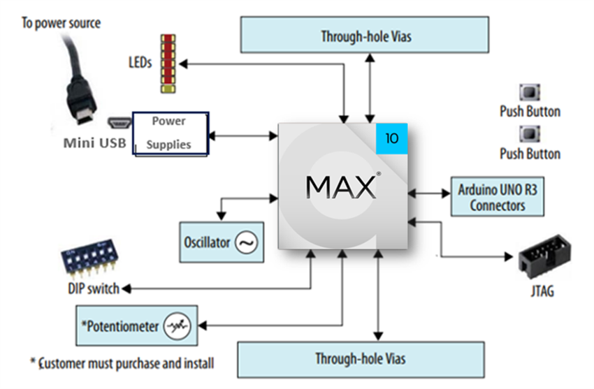
Key architectural highlights include the single-supply operation, which reduces power rail complexity, and the integrated analog-to-digital converter that eliminates the need for external ADC ICs in sensor-interface designs. The dual-configuration feature enables remote firmware updates with a safe fallback image, critical for deployed IoT and industrial systems.
3. Pinout & Package Information
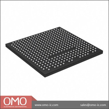
The 10M16SAU169I7G uses a 169-ball Ultra Fine-Pitch BGA (UBGA) package measuring 11 mm x 11 mm with a 0.8 mm ball pitch. This compact form factor is well-suited for space-constrained embedded systems. The package provides up to 130 user I/O pins, supporting a wide range of single-ended and differential I/O standards.

When designing the PCB layout for this device, ensure proper decoupling capacitors are placed close to the VCC and VCCIO power pins. Intel recommends a 4-layer or 6-layer PCB stack-up with dedicated power and ground planes for optimal signal integrity. The package features multiple I/O banks supporting mixed voltage levels (1.0 V to 3.3 V) per bank, dedicated analog pins (ANAIN1/ANAIN2) for the dual ADC, and standard JTAG interface pins (TCK, TMS, TDI, TDO) for programming and debug.
4. Typical Application Circuit
The 10M16SAU169I7G is commonly deployed in industrial automation, motor control, sensor fusion, and IoT edge computing applications. Below is a reference application showing the MAX 10 FPGA in a typical development/evaluation board configuration with DDR3 memory, analog inputs, and communication interfaces.
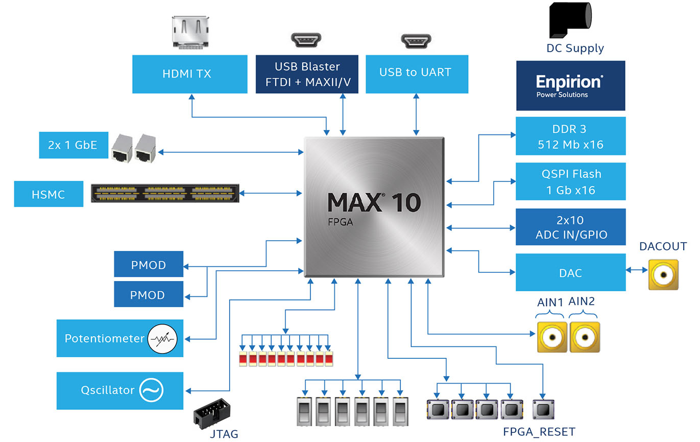
For a minimal design, the 10M16SAU169I7G requires only a single 3.3 V power supply, a few decoupling capacitors, and a JTAG header for programming. The integrated flash eliminates the external configuration PROM, and the on-chip ADC can directly interface with analog sensors, thermistors, or potentiometers. For more complex designs, the device supports DDR3 SDRAM interfaces for data buffering and high-speed LVDS I/O for inter-board communication.
Video Tutorial: Getting Started with MAX 10 FPGA
5. Ordering Information & Equivalents
The 10M16SAU169I7G is actively produced by Intel (formerly Altera) and is available through major authorized distributors. When ordering, verify the full part number suffix to ensure the correct package, temperature grade, and speed grade match your design requirements.
| Part Number | Temp Grade | Speed | Notes |
|---|---|---|---|
| 10M16SAU169I7G | Industrial (−40 to +100 °C) | 7 | This part – single supply, ADC, UBGA-169 |
| 10M16SAU169C8G | Commercial (0 to +85 °C) | 8 | Commercial temp variant |
| 10M16SCU169I7G | Industrial | 7 | Single supply, no ADC |
| 10M16DAU324I7G | Industrial | 7 | Dual supply, ADC, 324-ball UBGA |
| 10M16SAE144I7G | Industrial | 7 | Single supply, ADC, 144-pin EQFP |
Looking for related MAX 10 FPGA parts? Browse our catalog for more options:
- Shop All Altera / Intel FPGA Products at WWDParts
- Latest Semiconductor Technical Articles & Guides
- WWDParts – Your Trusted Electronic Components Distributor
6. FAQ – Frequently Asked Questions
Q1: What is the 10M16SAU169I7G and what family does it belong to?
The 10M16SAU169I7G is a non-volatile FPGA belonging to the Intel (Altera) MAX 10 family. It contains 16,000 logic elements, an integrated dual 12-bit ADC, and internal flash memory for instant-on configuration, all in a compact 169-ball UBGA package rated for industrial temperatures (−40 °C to +100 °C).
Q2: Does the 10M16SAU169I7G require an external configuration memory?
No. The MAX 10 family features integrated configuration flash memory on-chip, which means the FPGA powers up and configures itself instantly without needing an external PROM or SPI flash. This simplifies the BOM and board layout while enabling instant-on operation in under 10 ms.
Q3: What is the operating voltage for the 10M16SAU169I7G?
The 10M16SAU169I7G operates from a single 3.3 V power supply (range: 3.0 V to 3.6 V). The "S" in the part number denotes single-supply operation, which eliminates the need for separate core and I/O voltage rails found in dual-supply variants.
Q4: Can the 10M16SAU169I7G interface with DDR3 memory?
Yes. The MAX 10 10M16 device supports DDR3, DDR2, LPDDR2, and SRAM external memory interfaces through soft memory controller IP. Note that the U169 package has 130 user I/O pins, so DDR3 designs may be pin-constrained. Consider the larger F484 or U324 package variants for high-bandwidth memory applications.
Q5: What development tools are used to program the 10M16SAU169I7G?
The 10M16SAU169I7G is programmed using Intel Quartus Prime Lite Edition (free) or Standard Edition. Design entry supports VHDL, Verilog, and schematic capture. Programming is done via a USB-Blaster or USB-Blaster II JTAG cable. The Quartus toolchain also includes the Platform Designer (Qsys) for system integration and the Nios II soft processor for embedded applications.
Q6: What are the typical applications of the 10M16SAU169I7G?
Common applications include industrial motor control and drives, sensor hubs and data acquisition systems, IoT edge gateways, video surveillance pre-processing, medical instrumentation, portable test equipment, and automotive infotainment subsystems. The integrated ADC makes it especially attractive for analog-sensor-heavy designs that benefit from reduced BOM and board area.