10M16SAU169I7G Datasheet, Specifications & Application Guide – Altera MAX 10 FPGA
Overview of the 10M16SAU169I7G
The 10M16SAU169I7G is a non-volatile FPGA from the Altera (Intel) MAX 10 family, fabricated on TSMC's 55 nm embedded flash process. It integrates 16,000 logic elements, 549 Kb of M9K embedded SRAM, 2,368 Kb of user flash memory, 45 embedded 18×18 multipliers, and a dual 12-bit ADC — all on a single monolithic die. The device ships in a compact 169-ball UBGA package (11 mm × 11 mm) and is rated for the industrial temperature range of −40 °C to +100 °C.
The “SA” designation in the part number indicates single power supply with integrated analog (ADC) capability, making it an ideal single-chip solution that eliminates the need for an external configuration flash and a separate ADC IC. Configuration is stored in internal flash memory with dual-image support, enabling instant-on operation in under 10 ms and secure remote system updates (RSU) in the field.
The MAX 10 family is widely adopted across industrial control systems, motor drives, sensor hubs, IoT edge gateways, video surveillance pre-processing, medical instrumentation, and automotive ADAS front-end processing. If you are evaluating similar Altera FPGAs, you may also be interested in the 10M16SAU169C8G (commercial grade) or the 10M08SAE144C8G in the 144-EQFP package.
Key Specifications & Parameters
| Parameter | Value |
|---|---|
| Part Number | 10M16SAU169I7G |
| Family | MAX 10 (Altera / Intel) |
| Logic Elements (LEs) | 16,000 |
| Logic Array Blocks (LABs) | 1,000 |
| M9K Embedded Memory | 549 Kb (61 blocks) |
| User Flash Memory (UFM) | 2,368 Kb |
| 18 × 18 Multipliers | 45 |
| PLLs | 4 |
| Global Clock Networks | 16 |
| Max GPIO (device) | 320 |
| GPIO (U169 package) | 125 |
| LVDS Channels | 22 dedicated Tx / 151 Rx pairs |
| ADC | 1 block – dual 12-bit SAR, up to 1 MSPS, 17 analog inputs |
| Internal Configuration Images | 2 (dual-boot) |
| Process Technology | 55 nm TSMC Embedded Flash |
| Core Voltage (VCCINT) | 1.2 V |
| I/O Voltage | 1.0 V – 3.3 V (multi-volt) |
| Package | 169-ball UBGA, 11 mm × 11 mm, 0.8 mm pitch |
| Operating Temperature | −40 °C to +100 °C (Industrial) |
| Speed Grade | 7 |
| RoHS | Yes (suffix G) |
| EMIF Support | DDR3, DDR3L, DDR2, LPDDR2 up to 600 Mbps |
| Configuration Security | AES 128-bit encryption & compression |
Block Diagram & Architecture
The MAX 10 architecture arranges logic elements into LABs, each containing 16 adaptive LEs connected by a column-and-row routing fabric. M9K SRAM blocks (9 Kb each) line the interior columns for on-chip data buffering, while embedded 18×18 multiplier blocks sit adjacent for DSP-intensive workloads such as digital filtering and motor-control FOC algorithms. Four analog PLLs drive global and regional clock networks, and a dual 12-bit SAR ADC with an integrated temperature sensor occupies a dedicated analog column on the die.
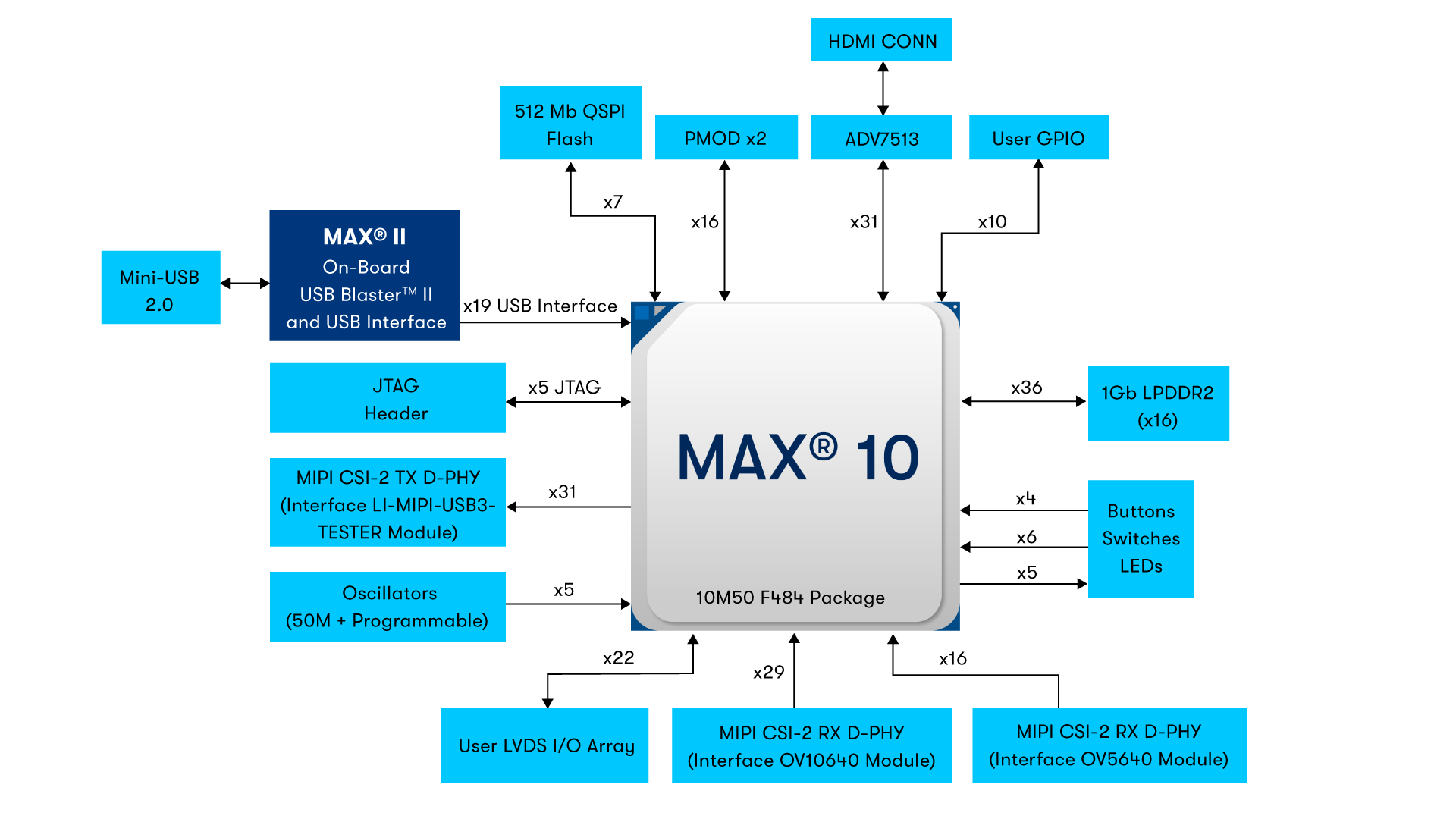
Figure 1: MAX 10 FPGA functional block diagram – logic array, embedded memory, DSP, PLL, and ADC blocks.
The internal flash stores up to two configuration images, enabling a safe dual-boot scheme: if a remote update to Image 1 fails, the device automatically falls back to the factory Image 0 at the next power cycle. This makes the 10M16SAU169I7G especially suited for field-deployed systems that require over-the-air firmware upgrades without physical access.
Pinout & Package Information
The 10M16SAU169I7G is housed in a 169-ball Ultra FineLine BGA (UBGA) package measuring 11 mm × 11 mm with a 0.8 mm ball pitch. It provides 125 user I/O pins across 8 I/O banks, supporting a wide range of single-ended standards (3.3 V LVTTL, 2.5 V / 1.8 V / 1.5 V LVCMOS) and differential pairs (LVDS at up to 720 Mbps). The compact UBGA footprint makes it well-suited for space-constrained designs on standard 4-layer PCBs.

Figure 2: 10M16SAU169I7G 169-UBGA package footprint and pinout layout.
The U169 package supports vertical migration to the 10M08 (8K LE) within the same footprint, allowing engineers to scale designs up or down without changing the PCB layout — a key advantage for product families with different feature tiers. For the complete pin table and bank assignments, refer to the official MAX 10 Pin-Out Files available from Altera.
Application Circuit & Design Guide
A typical application of the 10M16SAU169I7G combines its FPGA fabric, embedded ADC, and flash memory to create a single-chip sensor-hub controller. The ADC samples analog signals from external sensors (temperature, pressure, current), the FPGA fabric performs real-time signal conditioning and threshold monitoring, and the user flash stores calibration coefficients and event logs — all without any external memory or configuration device.
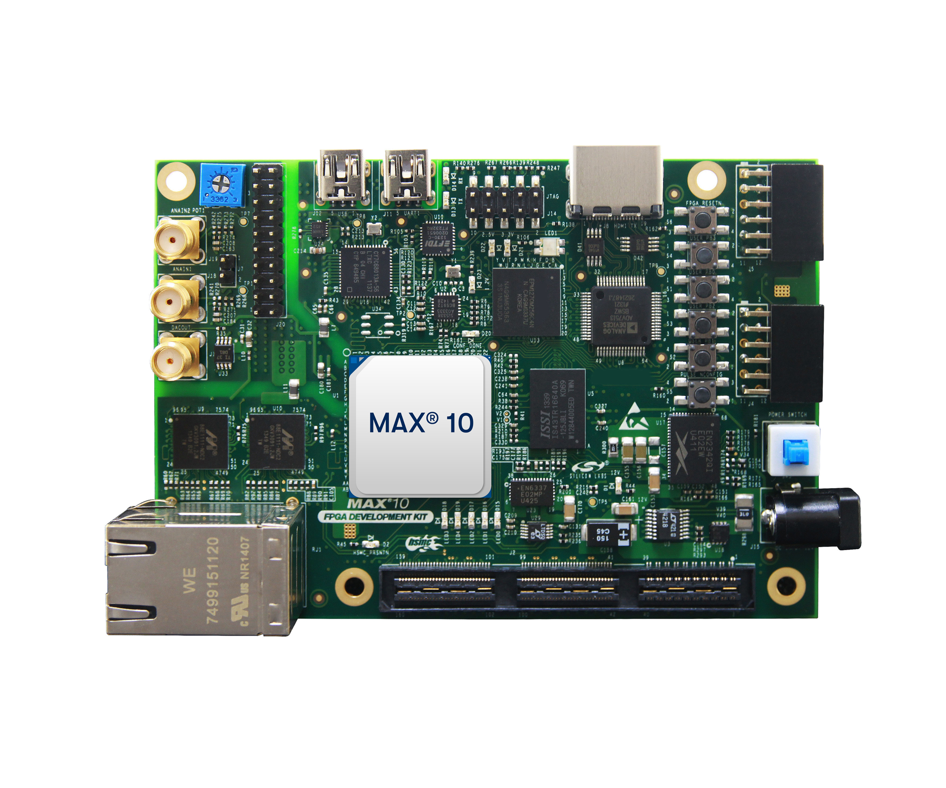
Figure 3: MAX 10 FPGA Development Kit – evaluation platform for prototyping 10M16SAU169I7G application circuits.
Design tips for the 10M16SAU169I7G:
- Power supply: As a single-supply (SA) variant, only a 3.3 V rail is required for both I/O and internal regulators. An internal 1.2 V core regulator simplifies the BOM.
- Decoupling: Place 100 nF ceramic capacitors on every VCC ball, plus bulk 10 µF capacitors near the device.
- ADC reference: For best ADC accuracy, provide a clean, low-noise 2.5 V or 3.3 V analog reference with a dedicated decoupling network.
- JTAG: Always connect the JTAG chain (TCK, TDI, TDO, TMS) with 1 kΩ pull-ups for reliable programming and debug via the USB-Blaster.
- DDR3 interface: The 10M16 in U169 supports external DDR3/DDR3L memory at up to 600 Mbps; follow the MAX 10 External Memory Interface User Guide for layout guidelines.
For development and prototyping, Altera offers the MAX 10 FPGA Evaluation Kit and the third-party Arrow DECA board, both of which feature the MAX 10 device family and include USB-Blaster, onboard ADC test points, and Pmod/GPIO headers. Explore more FPGA options on wwdparts.com FPGA collection.
Video Tutorial: Getting Started with MAX 10 FPGA
Frequently Asked Questions
What is the difference between the 10M16SAU169I7G and 10M16SAU169C8G?
Both devices share the same 16K LE silicon and U169 package. The key differences are: the I7G is rated for the industrial temperature range (−40 °C to +100 °C) with speed grade 7, while the C8G is rated for the commercial range (0 °C to +85 °C) with speed grade 8 (slower). Choose the I7G variant for harsh-environment or outdoor deployments.
Does the 10M16SAU169I7G require an external configuration flash?
No. The MAX 10 family stores its configuration bitstream in internal flash memory with support for two configuration images. This eliminates the cost and board space of an external serial configuration device (such as EPCS or EPCQ), and enables instant-on boot in under 10 ms.
How many I/O pins are available in the U169 package?
The 10M16 device in the U169 package provides 125 user I/O pins (out of 169 total balls). The maximum device GPIO count of 320 is only available in larger packages such as the F484. The U169 also supports 22 dedicated LVDS transmitter channels for high-speed differential signaling.
What ADC capabilities does the 10M16SAU169I7G offer?
The device integrates a dual 12-bit successive-approximation register (SAR) ADC with a cumulative sampling rate of up to 1 MSPS. It supports up to 17 analog input channels and includes an on-chip temperature sensor. The ADC is controlled through an Avalon-MM interface within the FPGA fabric, allowing seamless integration with Nios II soft processors or custom logic.
Can the 10M16SAU169I7G interface with DDR3 memory?
Yes. The 10M16 supports DDR3, DDR3L, DDR2, and LPDDR2 external memory interfaces at up to 600 Mbps through a hard memory controller IP. This is available in the U169 and larger packages. For best signal integrity, follow the layout guidelines in the MAX 10 External Memory Interface User Guide.
What design software is used to program the 10M16SAU169I7G?
The 10M16SAU169I7G is supported by Quartus Prime Lite Edition, which is available as a free download from Intel/Altera. It includes the full synthesis, place-and-route, timing analysis, and programming toolchain. For system-level design with a Nios II soft processor, use Platform Designer (formerly Qsys) and the Nios II Embedded Design Suite (EDS).
Looking for the 10M16SAU169I7G or other MAX 10 FPGAs? Browse our FPGA catalog or explore the full semiconductor blog for more datasheets, pinout guides, and application notes.