
10M08SAE144C8G Datasheet, Pinout, Specifications & Application Guide | Intel MAX 10 FPGA
The 10M08SAE144C8G is a versatile Intel MAX 10 FPGA featuring 8,000 logic elements, integrated ADC, and dual configuration flash in a compact 144-pin EQFP package. This comprehensive guide covers the complete datasheet specifications, pinout diagram, block diagram, application circuits, and frequently asked questions for engineers designing with this cost-effective, single-chip FPGA solution.
Table of Contents
1. 10M08SAE144C8G Overview & Key Features
The 10M08SAE144C8G belongs to Intel's MAX 10 FPGA family, built on a 55nm flash-based process technology. The "SA" in the part number designates a single-supply analog variant, meaning this device integrates an analog-to-digital converter (ADC) and operates from a single 3.3V power rail, simplifying board design and reducing BOM cost.
Key differentiators of the MAX 10 family include instant-on capability (no external configuration device required), dual configuration flash for seamless remote system upgrade, and user flash memory (UFM) for storing custom data. These features make the 10M08SAE144C8G ideal for system management, I/O expansion, motor control, and industrial automation applications.
Looking for other Intel FPGA solutions? Check out our guides on the wwdparts semiconductor blog for more FPGA and CPLD technical resources.
2. Detailed Specifications & Parameters
| Parameter | Value |
|---|---|
| Manufacturer | Intel (formerly Altera) |
| Family | MAX 10 (10M) |
| Part Number | 10M08SAE144C8G |
| Logic Elements (LEs) | 8,000 |
| LABs (Logic Array Blocks) | 500 |
| Embedded Memory (M9K) | 378 Kb (387,072 bits) |
| M9K Memory Blocks | 42 |
| User Flash Memory (UFM) | 32 KB |
| 18×18 Multipliers | 24 |
| PLLs | 2 |
| Global Clock Networks | 20 |
| Max User I/O Pins | 101 |
| Max LVDS Pairs | 15 |
| Integrated ADC | 1× 12-bit SAR ADC, up to 1 MSPS |
| ADC Channels | Up to 9 analog inputs |
| Configuration Flash | Dual-image internal flash |
| Core Voltage (VCCINT) | 1.2V |
| I/O Voltage (VCCIO) | 3.3V (2.85V–3.465V range) |
| Package Type | 144-EQFP (Enhanced Quad Flat Pack) |
| Package Dimensions | 20mm × 20mm |
| Pitch | 0.5mm |
| Mounting | Surface Mount (SMD) |
| Speed Grade | 8 |
| Temperature Range | Commercial: 0°C to 85°C (TJ) |
| Process Technology | 55nm Flash |
| RoHS Compliant | Yes (Lead-Free / Green) |
The 10M08SAE144C8G supports multiple I/O standards including 3.3V LVTTL, 1.0V–3.3V LVCMOS, SSTL, HSTL, and differential LVDS. The integrated Nios II soft-core processor enables embedded processing without an external MCU. For more semiconductor datasheets and specifications, visit our wwdparts component catalog.
3. Pinout Diagram & Package Information
The 10M08SAE144C8G uses a 144-pin EQFP package with an exposed thermal pad on the underside for enhanced heat dissipation. The 101 user I/O pins are organized into multiple I/O banks, each configurable for different voltage standards. Below is the package photograph showing the physical form factor:

The 144-EQFP package measures 20mm × 20mm with a 0.5mm pin pitch. Key power pins include VCCINT (1.2V core), VCCIO (3.3V I/O), and dedicated analog supply pins for the integrated ADC block. The exposed pad should be connected to ground for optimal thermal and electrical performance.
4. Block Diagram & Internal Architecture
The MAX 10 architecture integrates logic elements, embedded memory, DSP blocks, PLLs, ADC, and configuration flash into a single monolithic device. The block diagram below illustrates the major functional blocks:

The internal architecture features a column-based structure with logic array blocks (LABs), M9K embedded memory blocks, and 18×18 multiplier DSP blocks distributed across the fabric. The two PLLs provide flexible clock management with frequency synthesis and phase shifting. The dual configuration flash enables seamless firmware updates with automatic fallback to a known-good image.
5. Application Circuits & Design Examples
The 10M08SAE144C8G is widely used in industrial control, motor drives, communication bridges, and sensor interface applications. The Intel MAX 10 FPGA Evaluation Kit provides a ready-to-use development platform:
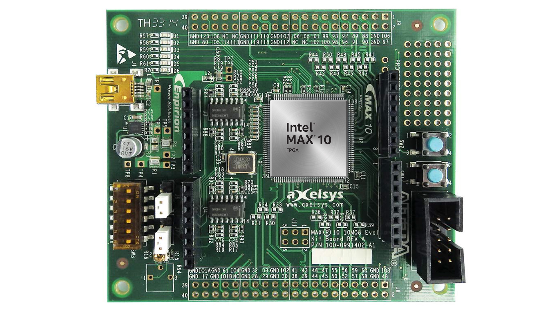
Typical application circuits leverage the single-supply design, requiring only a 3.3V input with internal LDOs generating the 1.2V core supply. The integrated ADC enables direct analog sensor interfacing without external ADC chips. Common design patterns include:
- System Management Controller: Monitoring power rails, fan speed, and temperature sensors via the integrated ADC
- Protocol Bridge: Converting between SPI, I2C, UART, and parallel interfaces using soft IP cores
- Motor Control: PWM generation with encoder feedback processing for BLDC and stepper motors
- IoT Edge Device: Sensor fusion with the Nios II processor and custom accelerators
For development, use Intel Quartus Prime Lite Edition (free) with the MAX 10 device support package. Explore more FPGA design resources at wwdparts.com.
Video Tutorial: Getting Started with Intel MAX 10 FPGA
6. Frequently Asked Questions (FAQ)
Q1: What is the difference between 10M08SAE144C8G and 10M08SCE144C8G?
The "SA" variant (10M08SAE144C8G) is a single-supply analog device with an integrated 12-bit ADC and operates from a single 3.3V supply with internal voltage regulators. The "SC" variant is a single-supply compact device without the ADC block. Choose the SA variant when you need analog-to-digital conversion capabilities on-chip.
Q2: Does the 10M08SAE144C8G require an external configuration memory?
No. The MAX 10 family features internal configuration flash memory, enabling instant-on operation without any external configuration PROM, EPCS, or EPCQ device. The device stores up to two configuration images internally, supporting dual-boot and remote system upgrade functionality.
Q3: What development tools are needed for the 10M08SAE144C8G?
You need Intel Quartus Prime Lite Edition (free download, no license required) for synthesis, place-and-route, and programming. For programming hardware, use an Intel USB-Blaster or USB-Blaster II download cable via JTAG. The Nios II Embedded Design Suite is included for soft-core processor development.
Q4: What is the maximum operating frequency of the 10M08SAE144C8G?
The speed grade 8 device supports logic fabric speeds up to approximately 300 MHz for register-to-register paths (depending on design complexity). The internal oscillator runs at up to 232 MHz. The integrated ADC supports sampling rates up to 1 MSPS (million samples per second).
Q5: Can the 10M08SAE144C8G be used in automotive applications?
The "C" temperature grade (0°C to 85°C) is suitable for consumer and industrial applications. For automotive use, select the "I" (industrial: -40°C to 100°C) or "A" (automotive: -40°C to 125°C) temperature grade variants. Intel offers AEC-Q100 qualified versions of MAX 10 for automotive applications.
Q6: How much power does the 10M08SAE144C8G consume?
Typical static power consumption is approximately 45–55 mW in standby mode. Dynamic power varies with operating frequency, toggle rate, and resource utilization. Use the Intel Early Power Estimator (EPE) spreadsheet tool to calculate power for your specific design. The single-supply architecture simplifies power distribution and reduces total system power compared to multi-rail FPGA solutions.


