10M16SAU169I7G Datasheet, Specifications & Application Guide – Altera MAX 10 FPGA
Overview of the 10M16SAU169I7G
The 10M16SAU169I7G is a non-volatile FPGA from the Altera (Intel) MAX 10 family, fabricated on a 55 nm flash process. It integrates 16,000 logic elements, a dual 12-bit analog-to-digital converter (ADC), and internal configuration flash memory—enabling instant-on operation without an external configuration device. The "I7G" suffix designates industrial-grade temperature range (−40 °C to +100 °C) and speed grade 7, making it ideal for harsh-environment embedded systems.
MAX 10 FPGAs are unique in combining non-volatile configuration storage, an analog-to-digital converter, and a compact single-chip solution, eliminating the need for external flash or EEPROM. This simplifies board design and reduces BOM cost while maintaining the flexibility and parallel processing power inherent in FPGA architectures.
Key Specifications & Parameters
| Parameter | Value |
|---|---|
| Part Number | 10M16SAU169I7G |
| Family | MAX 10 (Altera / Intel) |
| Logic Elements (LEs) | 16,000 |
| Logic Array Blocks (LABs) | 1,000 |
| Embedded Memory | 549 Kb (M9K blocks) |
| User Flash Memory (UFM) | 2,368 Kb |
| 18×18 Multipliers | 45 |
| PLLs | 4 |
| ADC | Dual 12-bit, 1 MSPS |
| Maximum User I/Os | 130 |
| Maximum LVDS Pairs | 22 |
| Package | 169-ball UBGA (11×11 mm) |
| Core Voltage | 1.2 V |
| I/O Voltage | 3.0 V / 3.3 V |
| Operating Temperature | −40 °C to +100 °C (Industrial) |
| Speed Grade | 7 |
| Process Node | 55 nm |
| Configuration | Internal Flash (instant-on) |
| I/O Standards | LVTTL, LVCMOS, SSTL, HSTL, LVDS, RSDS, mini-LVDS |
Pinout, Package & Block Diagram
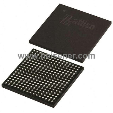
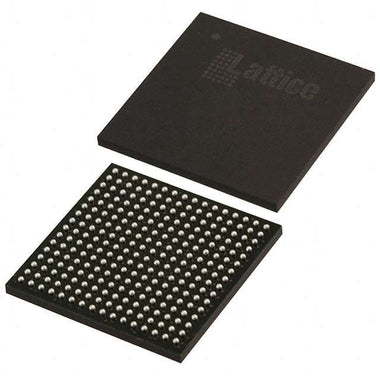
The 10M16SAU169I7G is housed in a compact 169-ball UBGA package measuring 11×11 mm with a 0.8 mm ball pitch. The pinout provides 130 user I/O pins supporting multiple I/O voltage standards from 1.0 V to 3.3 V, four PLL clock inputs, dedicated JTAG programming pins, and analog input channels for the integrated ADC block.


Typical Applications & Design Examples
The combination of instant-on flash configuration, integrated ADC, and industrial temperature support makes the 10M16SAU169I7G a versatile choice for a wide range of embedded applications:
- Industrial Automation & Motor Control: Real-time PWM generation, encoder interfaces, and sensor fusion with the built-in ADC for current sensing.
- IoT Edge Gateways: Protocol bridging (SPI, I²C, UART, Ethernet) with hardware acceleration for edge computing tasks.
- Medical Instrumentation: Signal conditioning and data acquisition leveraging the 12-bit ADC for patient monitoring devices.
- Video & Image Processing: Pre-processing pipelines for surveillance cameras and machine vision systems.
- Test & Measurement: Custom digital logic for laboratory instruments requiring deterministic timing.
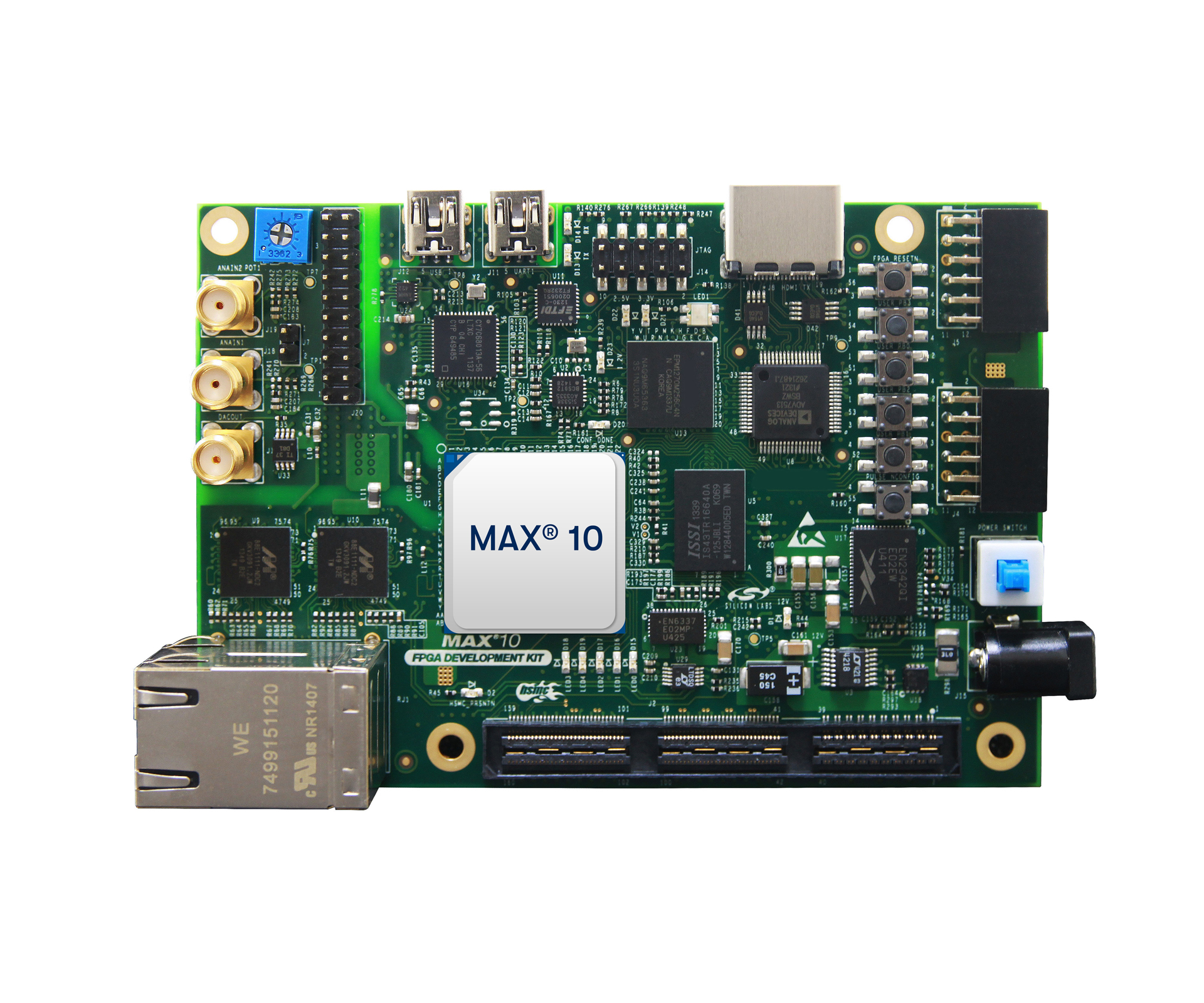
Development tools include the free Quartus Prime Lite Edition, which provides synthesis, place-and-route, timing analysis, and JTAG programming support. Popular development boards such as the Terasic DE10-Lite and the Arrow MAX1000 feature MAX 10 FPGAs with on-board USB-Blaster programming, SDRAM, VGA output, and Arduino-compatible headers for rapid prototyping.
Video Tutorial: Getting Started with MAX 10 FPGA
Ordering & Availability at WWDParts
The 10M16SAU169I7G is available for immediate purchase at WWDParts.com with competitive pricing and fast worldwide shipping. We maintain stock of the full MAX 10 family to support your production and prototyping needs.
Related parts you may also need:
- 10M16SAU169C8G – Commercial-grade variant (0 °C to +85 °C)
- 10M08SAE144C8G – 8K LE MAX 10 in 144-pin EQFP
- 10M04SCE144C8G – 4K LE MAX 10 for cost-sensitive designs
Frequently Asked Questions
What is the difference between the 10M16SAU169I7G and 10M16SAU169C8G?
The 10M16SAU169I7G is the industrial-grade variant with an extended operating temperature range of −40 °C to +100 °C and speed grade 7, while the 10M16SAU169C8G is the commercial-grade version rated for 0 °C to +85 °C with speed grade 8. Choose the I7G for applications exposed to extreme temperatures such as outdoor industrial equipment or automotive subsystems.
Does the 10M16SAU169I7G require an external configuration memory?
No. The MAX 10 family features internal flash-based configuration memory, providing instant-on operation. The FPGA boots from its internal flash within milliseconds of power-up, eliminating the need for external EEPROM or SPI flash devices and reducing board complexity.
How do I use the integrated ADC on the 10M16SAU169I7G?
The dual 12-bit ADC is accessed through a dedicated IP core in the Quartus Prime software. You instantiate the "Modular ADC Core" IP, configure the analog channels and sampling rate (up to 1 MSPS), and connect it to your FPGA logic. The ADC supports up to 18 analog input channels routed from dedicated analog pins on the package.
What development board supports the 10M16SAU169I7G?
While the exact 10M16SAU169I7G part is not mounted on most eval boards, the Terasic DE10-Lite (10M50DAF484) and the Arrow MAX1000 (10M08SAU169) share the same MAX 10 architecture and Quartus Prime toolchain. Designs created on these boards can be directly ported to the 10M16SAU169I7G with minimal pin reassignment.
What is the maximum operating frequency of the 10M16SAU169I7G?
The maximum clock frequency depends on your specific design's timing paths. The four on-chip PLLs support input frequencies from 5 MHz to 472.5 MHz and can generate output clocks up to 472.5 MHz. Typical user logic achieves 150–250 MHz depending on design complexity and optimization settings in Quartus Prime.
Can I use the 10M16SAU169I7G for dual-boot or remote system upgrade?
Yes. The MAX 10 internal flash supports dual configuration images, enabling a safe remote system upgrade (RSU) workflow. The application image is stored alongside a factory-safe image. If the new image fails, the device automatically falls back to the factory image on the next power cycle, ensuring field-deployed systems remain operational.