
10M16SAU169I7G Datasheet, Specifications & Application Guide – Altera MAX 10 FPGA
The 10M16SAU169I7G is a non-volatile FPGA from the Altera (Intel) MAX 10 family, built on a 55 nm process node. It integrates 16,000 logic elements, a dual 12-bit ADC, 549 Kb of embedded SRAM, and 2,304 Kb of user flash memory into a compact 169-ball UBGA package. With single-supply operation, instant-on boot from internal flash, and an industrial temperature rating of −40 °C to +100 °C, the 10M16SAU169I7G is an ideal choice for cost-sensitive embedded and mixed-signal applications.
Table of Contents
- 1. Overview & Part Number Decoding
- 2. Key Specifications & Parameters
- 3. Block Diagram & Architecture
- 4. Pinout, Package & Footprint
- 5. Typical Applications & Design Resources
- 6. Frequently Asked Questions (FAQ)
1. Overview & Part Number Decoding
The part number 10M16SAU169I7G decodes as follows:
- 10M16 – MAX 10 family, 16K logic elements
- S – Single power-supply mode (integrated 1.2 V core regulator)
- A – Analog block enabled (dual 12-bit ADC)
- U169 – 169-ball UBGA (Micro Fine-pitch Ball Grid Array) package
- I – Industrial temperature range (−40 °C to +100 °C)
- 7 – Speed grade 7
- G – Lead-free / RoHS-compliant packaging
The MAX 10 family is unique among FPGAs for its non-volatile, single-chip architecture: configuration data is stored in on-die flash, eliminating the need for an external configuration PROM and enabling instant-on operation with deterministic boot times under 10 ms.
2. Key Specifications & Parameters
| Parameter | Value |
|---|---|
| Manufacturer | Altera (Intel) |
| Family | MAX 10 FPGA |
| Logic Elements (LEs) | 16,000 |
| Logic Array Blocks (LABs) | 1,000 |
| Embedded SRAM (M9K) | 549 Kb |
| User Flash Memory (UFM) | 2,304 Kb |
| 18x18 DSP Multiplier Blocks | 45 |
| PLLs | 4 |
| ADC | Dual 12-bit, up to 1 MSPS |
| Maximum User I/O | 130 |
| Maximum LVDS Pairs | 22 |
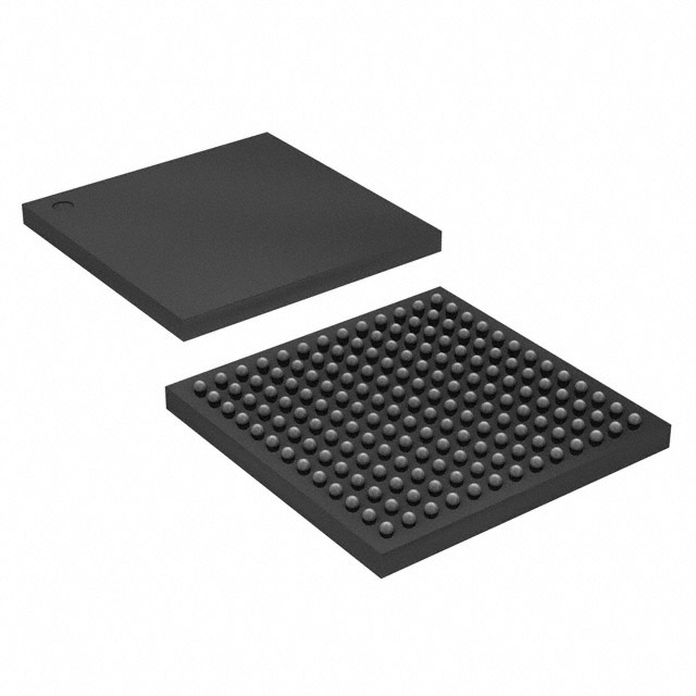
| Package | 169-ball UBGA (11 x 11 mm) |
| Supply Voltage | 3.3 V single supply (internal 1.2 V regulator) |
| I/O Standards | 3.3 V / 2.5 V / 1.8 V / 1.5 V LVCMOS/LVTTL, SSTL, HSTL, HSUL, LVDS |
| External Memory Interface | DDR3, DDR2, LPDDR2, SRAM |
| Configuration | Internal flash (instant-on), JTAG, AS |
| Operating Temperature | -40 C to +100 C (Industrial) |
| Speed Grade | 7 |
| Process Technology | 55 nm |
| RoHS Compliant | Yes |
3. Block Diagram & Architecture
The MAX 10 architecture combines programmable logic, memory, DSP, and analog capabilities in a single monolithic die. The diagram below illustrates the key functional blocks of the MAX 10 development platform, showing how the FPGA interfaces with external peripherals.
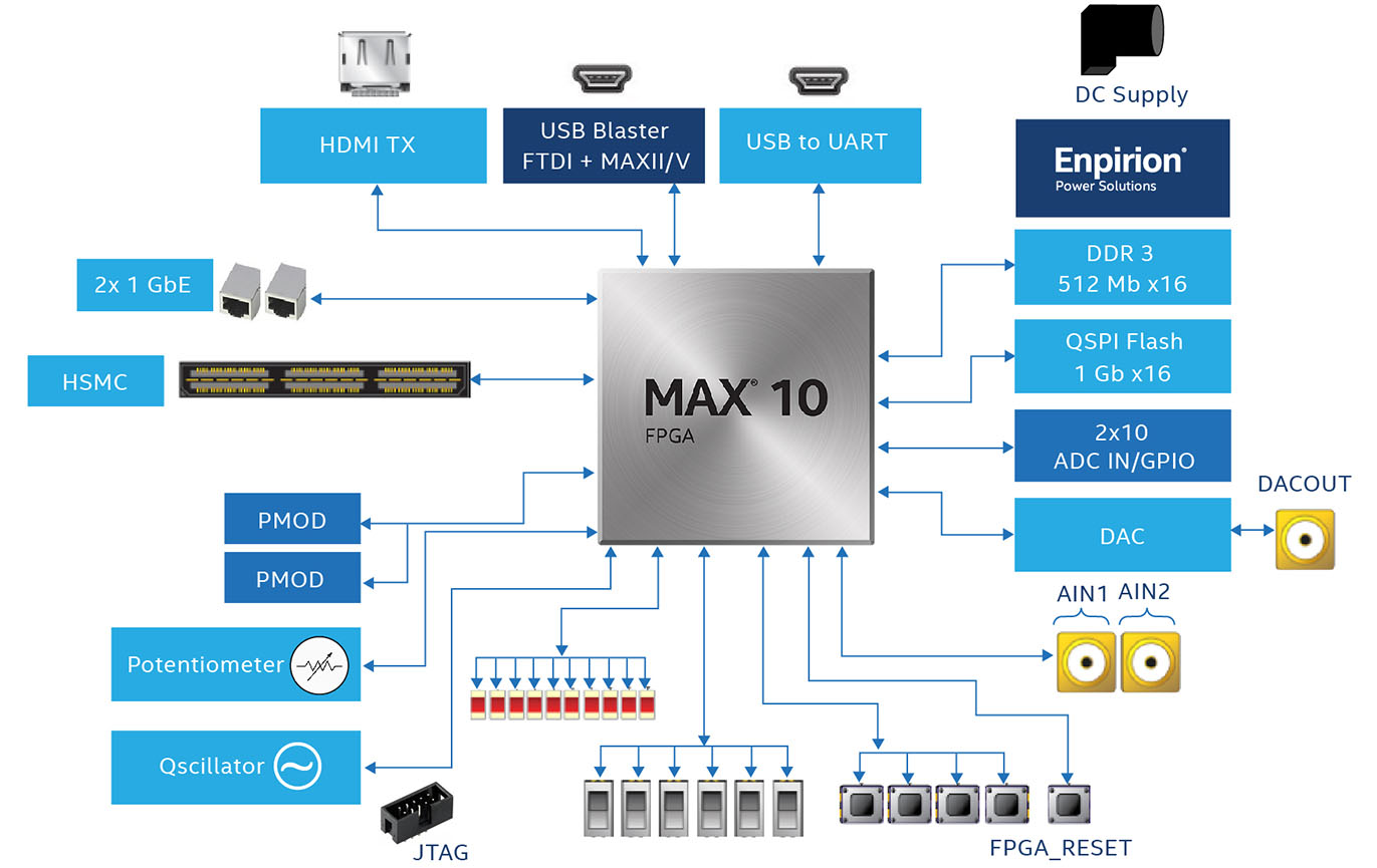
Key architectural highlights include four fabric PLLs supporting clock management up to 500 MHz, M9K embedded memory blocks configurable as single- or dual-port RAM, ROM, or FIFO, and a dual 12-bit ADC with up to 18 analog input channels. The internal flash configuration memory supports dual-image storage for safe remote firmware updates.
4. Pinout, Package & Footprint
The 10M16SAU169I7G uses the U169 UBGA package — a 169-ball micro fine-pitch BGA with a 0.8 mm ball pitch in a compact 11 x 11 mm body. Of the 169 balls, 130 are available as user I/O, organized across multiple I/O banks supporting a variety of single-ended and differential standards.
For PCB design, schematic symbols and verified footprints are available from SnapEDA. Pin-out files in PDF, XLS, and TXT formats can be downloaded from the official Altera pin-out page.
5. Typical Applications & Design Resources
The combination of instant-on configuration, integrated ADC, and compact single-supply packaging makes the 10M16SAU169I7G well-suited for a wide range of embedded applications:
- Industrial control & motor drives – Real-time PWM generation, encoder interfaces, and sensor fusion with on-chip ADC
- IoT edge gateways & sensor hubs – Protocol bridging (SPI, I2C, UART), data aggregation, and low-latency preprocessing
- Video surveillance preprocessing – Frame buffering with DDR3 interface, image scaling, and overlay generation
- Medical instrumentation – Analog signal acquisition via dual ADC, digital filtering, and deterministic timing
- Test & measurement equipment – High-speed data capture and custom digital protocol decoding
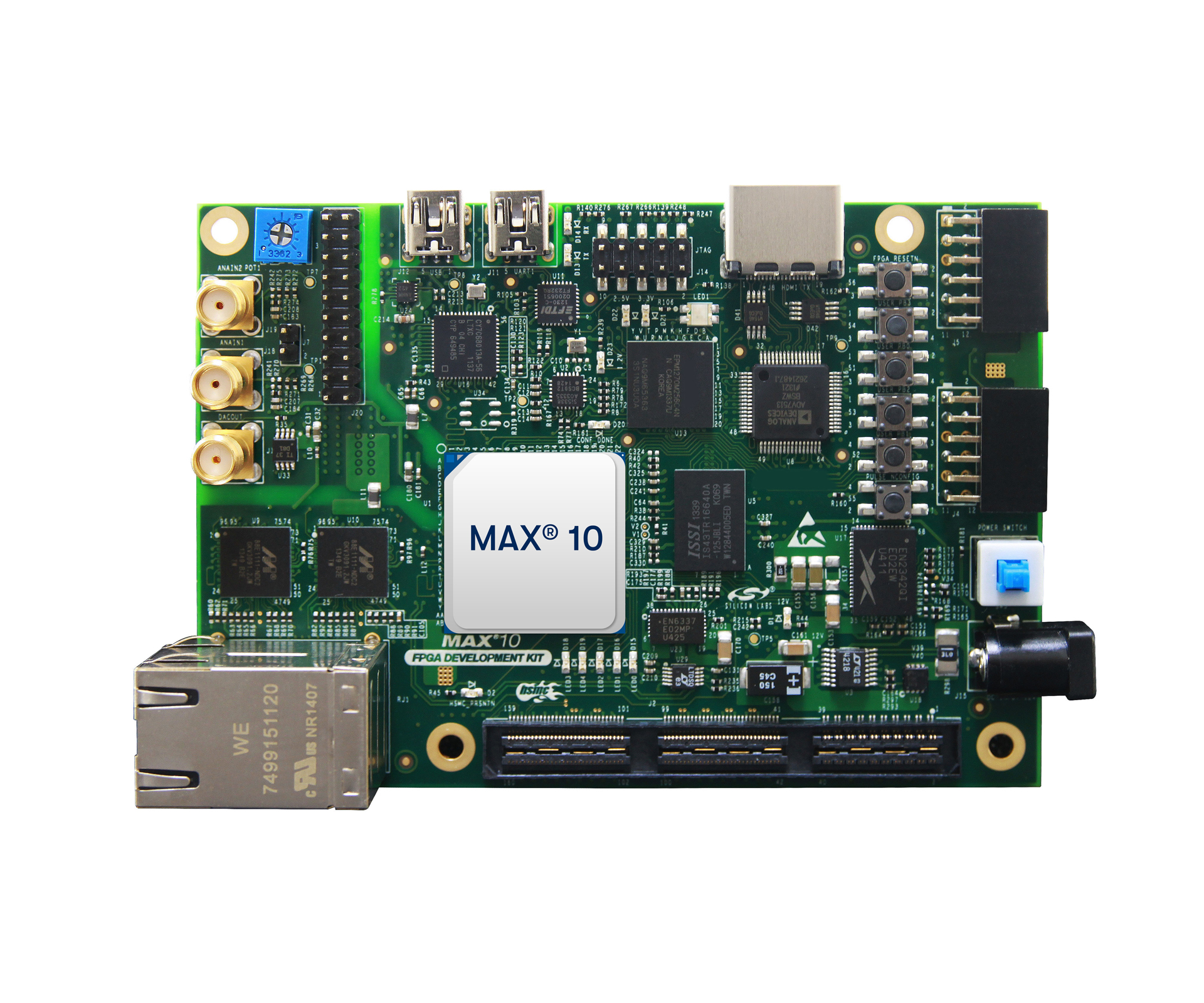
The MAX 10 FPGA Development Kit provides a ready-made evaluation platform with DDR3 memory, HSMC expansion, and built-in USB Blaster II programmer. All MAX 10 designs are developed using Quartus Prime Lite Edition (free), which includes full synthesis, place-and-route, timing analysis, and in-system programming support.
Looking for related Altera MAX 10 parts? Browse our selection:
- 10M16SAU169C8G – MAX 10 16K LE, U169, Commercial Grade
- Altera FPGA & CPLD Collection at WWDParts
- All FPGA Products at WWDParts
Video Tutorial: Getting Started with MAX 10 FPGA
6. Frequently Asked Questions (FAQ)
What is the 10M16SAU169I7G?
The 10M16SAU169I7G is a non-volatile FPGA from the Altera (Intel) MAX 10 family. It features 16,000 logic elements, a dual 12-bit ADC, 549 Kb of embedded SRAM, and 2,304 Kb of user flash memory in a 169-ball UBGA package, rated for industrial temperatures (-40 C to +100 C).
What is the difference between the 10M16SAU169I7G and 10M16SAU169C8G?
Both share the same 16K LE die and U169 package. The key differences are temperature range and speed grade: the I7G variant is rated for industrial temperatures (-40 C to +100 C) at speed grade 7, while the C8G variant is rated for commercial temperatures (0 C to +85 C) at speed grade 8.
Does the 10M16SAU169I7G require an external configuration memory?
No. The MAX 10 family stores its configuration bitstream in on-die flash memory, enabling instant-on operation without any external PROM or flash chip. It also supports dual-image configuration for safe remote updates.
What software tools are needed to program the 10M16SAU169I7G?
You need Quartus Prime Lite Edition (free from Intel/Altera), which provides full synthesis, fitting, timing analysis, and programming support for all MAX 10 devices. Programming is done via JTAG or Active Serial (AS) using a USB Blaster cable.
What is the ADC specification of the 10M16SAU169I7G?
The device integrates a dual 12-bit successive-approximation ADC with a maximum sample rate of 1 MSPS. It supports up to 18 analog input channels, making it ideal for mixed-signal applications that require on-chip analog-to-digital conversion without external ADC ICs.
Can the 10M16SAU169I7G interface with DDR3 memory?
Yes. The MAX 10 family supports DDR3, DDR2, LPDDR2, and SRAM external memory interfaces. The device includes dedicated I/O circuitry and calibration logic for reliable high-speed memory operation, although it does not include a hard memory controller — the controller is implemented in programmable logic.


