
10M16SAU169I7G Datasheet, Specifications & Application Guide – Altera MAX 10 FPGA
The 10M16SAU169I7G is a high-performance FPGA from the Intel (Altera) MAX 10 family, offering 16,000 logic elements in a compact 169-ball UBGA package. Featuring an integrated dual ADC, internal flash configuration memory, and instant-on capability, this device is ideal for industrial IoT, motor control, sensor fusion, and edge computing applications.
Overview & Key Features
The 10M16SAU169I7G belongs to the Intel MAX 10 FPGA series, manufactured on a 55 nm process node. The industrial-grade temperature rating ensures reliable operation from -40 to +100 degrees C.
- Instant-on operation - Internal flash configuration memory eliminates external configuration devices.
- Integrated dual 12-bit ADC - Up to 18 analog input channels with 1 MSPS conversion rate.
- Low power consumption - Single 3.3 V supply operation.
- Rich I/O support - LVDS, LVCMOS, SSTL, HSTL, and PCI-compliant I/O standards.
- DDR memory interfaces - Native support for DDR3, DDR2, and LPDDR2 external memory.
Technical Specifications
| Parameter | Value |
|---|---|
| Part Number | 10M16SAU169I7G |
| Manufacturer | Intel (Altera) |
| Family | MAX 10 FPGA |
| Logic Elements (LEs) | 16,000 |
| Logic Array Blocks (LABs) | 1,000 |
| Embedded SRAM | 549 Kb |
| User Flash Memory (UFM) | 2,304 Kb |
| DSP Blocks (18x18 Multipliers) | 45 |
| PLLs | 4 |
| Analog-to-Digital Converter | Dual 12-bit ADC, up to 1 MSPS |
| Maximum User I/O | 130 (U169 package) |
| Maximum LVDS Pairs | 22 |
| Package | 169-ball UBGA (11 x 11 mm) |
| Supply Voltage | 3.0 V - 3.3 V |
| Operating Temperature | -40 C to +100 C (Industrial) |
| Speed Grade | 7 |
| Process Technology | 55 nm |
| External Memory Interface | DDR3, DDR2, LPDDR2, SRAM |
| I/O Standards | LVTTL, LVCMOS (1.0-3.3 V), PCI, SSTL, HSTL, LVDS |
| Configuration | Internal flash (instant-on), dual boot images |
| Lead-Free / RoHS | Yes (Green / G suffix) |
Block Diagram & Architecture
The MAX 10 architecture integrates programmable logic, embedded memory, DSP blocks, PLLs, a dual ADC, and user flash memory on a single die.

The logic array consists of 1,000 LABs. Embedded memory blocks provide 549 Kb of SRAM. The 45 DSP blocks support high-throughput multiply-accumulate operations.
Pinout & Package Information
The 10M16SAU169I7G is housed in a 169-ball UBGA package with an 11 x 11 mm body size and 0.8 mm ball pitch.
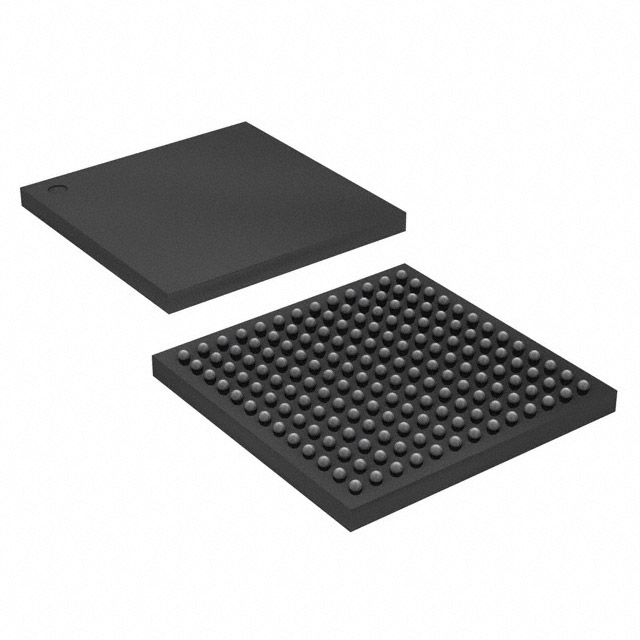
The U169 package provides up to 130 user I/O pins organized across multiple I/O banks. Dedicated pins include JTAG, configuration pins, analog input channels for the ADC, and power/ground connections.
Application Circuit & Design Guide
The 10M16SAU169I7G is deployed across industrial automation, motor drives, video surveillance, IoT edge gateways, and medical instrumentation.
Power Supply Design
A single 3.3 V supply powers the core logic and I/O banks. Decouple each VCC pin with 100 nF ceramic capacitors placed close to the BGA pads, and add bulk 10 uF capacitors per power rail.
Clock & PLL Configuration
Use a 50 MHz crystal oscillator connected to a dedicated clock input pin. The four on-chip PLLs can generate multiple clock domains up to 500 MHz internal.
ADC Integration
The dual 12-bit ADC supports up to 18 analog input channels with a 0-3.3 V input range. Use external anti-aliasing RC filters on each analog input. Configure via Quartus Platform Designer (Qsys).
Configuration & Programming
Program through JTAG using an Intel USB Blaster. The internal flash stores up to two configuration images with automatic fallback. No external flash or CPLD is required.
Recommended Development Tools
- Intel Quartus Prime Lite Edition (free) - Full synthesis, place-and-route, and timing analysis.
- Platform Designer (Qsys) - System integration for Nios II soft-processor, ADC controller, and memory interfaces.
- ModelSim Intel FPGA Edition - RTL and gate-level simulation.
Video Tutorial
Watch this getting-started tutorial for the Intel MAX 10 FPGA evaluation kit:
Frequently Asked Questions
What is the 10M16SAU169I7G?
The 10M16SAU169I7G is a 16,000-logic-element FPGA from the Intel (Altera) MAX 10 family with integrated dual 12-bit ADC, internal flash configuration, 549 Kb SRAM, 45 DSP blocks, and 130 I/O pins in a 169-ball UBGA package.
What is the difference between 10M16SAU169I7G and 10M16SAU169C8G?
The I7 variant is rated for industrial temperature (-40 to +100 C) with speed grade 7, while the C8 variant is rated for commercial range (0 to +85 C) with speed grade 8.
Does the 10M16SAU169I7G require an external configuration device?
No. The MAX 10 includes on-chip flash configuration memory storing up to two images, enabling instant-on without external flash or CPLD.
How do I use the integrated ADC on the 10M16SAU169I7G?
Configure the dual 12-bit ADC via Platform Designer (Qsys) in Quartus Prime. Add the Modular ADC Core IP, select analog channels (up to 18), set the sampling rate (up to 1 MSPS), and connect via Avalon-MM interface.
What development tools do I need for the 10M16SAU169I7G?
Intel Quartus Prime Lite Edition (free) for synthesis and programming, an Intel USB Blaster for JTAG configuration, and ModelSim for simulation.
What are the main applications for the 10M16SAU169I7G?
Industrial motor control, IoT sensor hubs, video surveillance, medical instrumentation, building automation, and portable test equipment.
Looking for more FPGA and semiconductor components? Explore our catalog:


