
1. 10M04SCE144C8G Overview
The 10M04SCE144C8G is an Intel (formerly Altera) MAX 10 FPGA built on 55nm non-volatile process technology. It belongs to the single-supply, compact (SC) variant of the MAX 10 family, offering 4,000 logic elements in a space-efficient 144-pin EQFP package. Unlike the SA variants, the SC series omits the on-chip ADC block, making it an ideal cost-optimized solution for pure digital logic applications.
Designed for instant-on operation with internal configuration flash memory, the 10M04SCE144C8G eliminates the need for an external configuration device. This makes it particularly attractive for industrial control systems, IoT edge devices, motor drive interfaces, and communication protocol bridging where board space and BOM cost are critical constraints.
If you are evaluating similar devices in the MAX 10 family, you may also be interested in the 10M08SAE144C8G (8K LE with ADC) or the 10M16SAU169C8G (16K LE in U169 package).
2. Key Specifications & Parameters
| Parameter | Value |
|---|---|
| Manufacturer | Intel (Altera) |
| Family | MAX 10 FPGA |
| Logic Elements (LEs) | 4,000 |
| Embedded Memory | 189 Kb (M9K blocks) |
| User Flash Memory (UFM) | Yes |
| Phase-Locked Loops (PLLs) | 2 |
| User I/O Pins | 101 (E144 package) |
| ADC Block | No (SC variant) |
| Max Clock Frequency | ~402 MHz |
| Package | 144-EQFP (20 × 20 mm) |
| Core Voltage | 1.2 V (single supply) |
| I/O Voltage | 3.0 V – 3.3 V |
| I/O Standards | LVTTL, LVCMOS, LVDS, SSTL, PCI |
| Speed Grade | 8 |
| Temperature Range | 0 °C to +85 °C (Commercial) |
| Process Technology | 55 nm |
| Configuration | Internal Flash (dual-image), JTAG |
| RoHS Compliant | Yes (Lead-Free / Green) |
3. Pinout & Package Information
The 10M04SCE144C8G is housed in a 144-pin EQFP (Enhanced Quad Flat Package) with an exposed thermal pad on the underside. The package measures 20 × 20 mm with a 0.5 mm lead pitch, providing 101 user-configurable I/O pins organized across four I/O banks.

Figure 1: 10M04SCE144C8G in 144-EQFP package (Image: DigiKey)
Each I/O bank supports multiple voltage standards (1.2 V to 3.3 V LVCMOS/LVTTL), and up to 15 LVDS differential pairs are available for high-speed serial interfaces. The exposed pad should be connected to ground for optimal thermal and electrical performance. For the full pin assignment table, refer to the 10M04SCE144C8G detailed pinout guide.
4. Block Diagram & Internal Architecture
The MAX 10 architecture integrates several key functional blocks into a single monolithic die:
- Logic Array Blocks (LABs) – Each LAB contains 16 Adaptive Logic Modules (ALMs), providing the core programmable logic fabric.
- M9K Embedded Memory – 189 Kb of dual-port SRAM organized in 9 Kb blocks, supporting various memory configurations (ROM, single/dual-port RAM, FIFO).
- Configuration Flash Memory (CFM) – Stores up to two compressed configuration images for instant-on and remote update capability.
- User Flash Memory (UFM) – Non-volatile storage accessible via Avalon-MM interface, ideal for storing calibration data, serial numbers, or small lookup tables.
- PLLs – Two general-purpose PLLs with up to five output counters each, supporting frequency synthesis, clock multiplication, and phase shifting.
- I/O Elements (IOEs) – Programmable I/O cells with DDR support, programmable drive strength, and on-chip termination.
Figure 2: Intel MAX 10 FPGA architecture overview (Image: RayPCB)
5. Application Circuit & Design Guide
The 10M04SCE144C8G is well-suited for a wide range of embedded applications. Below are typical use cases and design considerations:
Typical Applications
- Industrial Automation – Servo motor control, PLC I/O expansion, sensor aggregation
- IoT Edge Processing – Protocol conversion (SPI/I2C/UART bridging), data preprocessing before cloud upload
- Communication Infrastructure – Clock recovery, LVDS serializer/deserializer, line coding
- Consumer Electronics – LED display controllers, keyboard scan matrices, audio signal routing
- Power Management – Digital power sequencing, voltage monitoring, PMBus interface logic
Power Supply Design
The SC variant requires only a single 1.2 V core supply (VCCINT), significantly simplifying the power tree. I/O banks are powered at 3.3 V (VCCIO). A typical design uses a single LDO or DC-DC converter from a 5 V or 3.3 V system rail. Decoupling capacitors (100 nF ceramic + 10 µF bulk) should be placed close to each VCC pin.
Development Environment
Intel Quartus Prime Lite Edition (free) provides full synthesis, simulation, and programming support for all MAX 10 devices. Configuration is performed via JTAG using a USB-Blaster or compatible programmer.
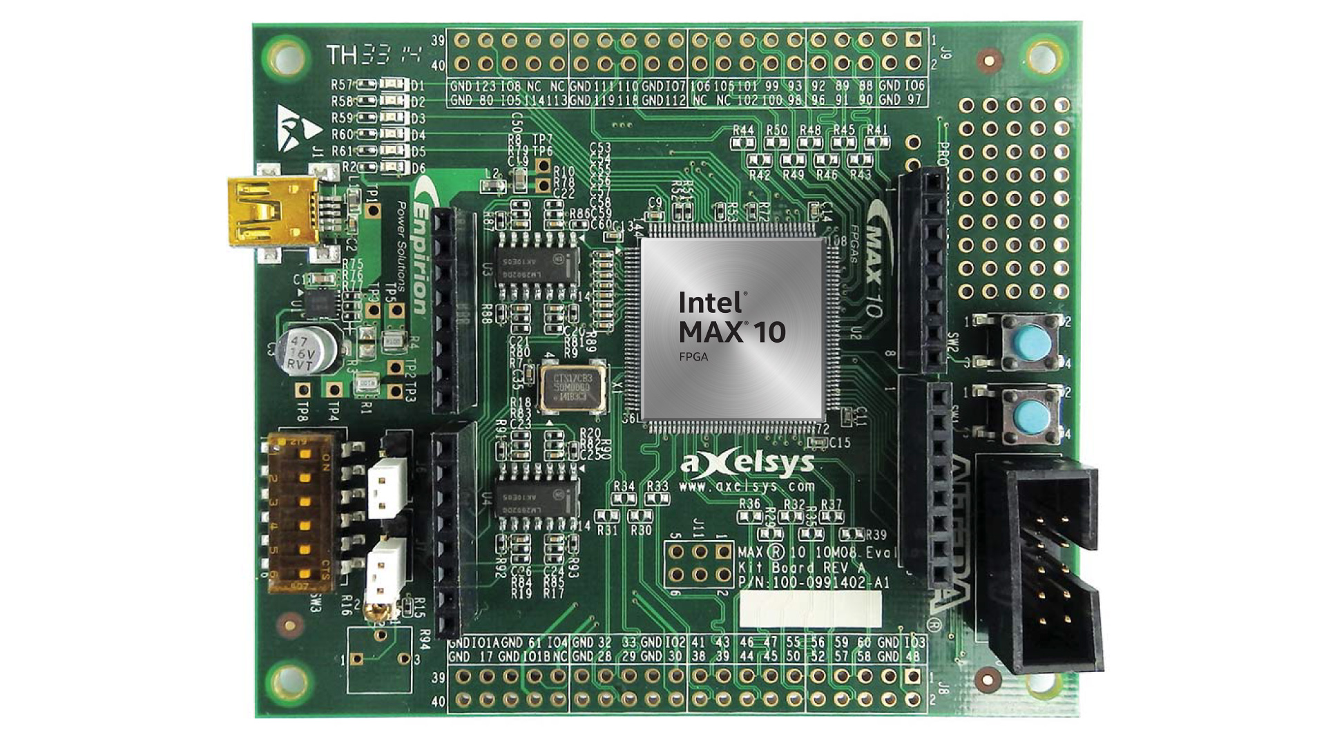
Figure 3: MAX 10 FPGA Evaluation Kit for rapid prototyping (Image: Altera/Intel)
Video Tutorial: Getting Started with MAX 10 FPGA
Video: FPGA Software and First Example for Altera/Intel MAX 10 Development Kit
6. FAQ – Frequently Asked Questions
Q1: What is the difference between 10M04SCE144C8G and 10M04SAE144C8G?
The key difference is the ADC block. The SC variant (10M04SCE144C8G) does not include an on-chip analog-to-digital converter, while the SA variant (10M04SAE144C8G) integrates a dual 12-bit ADC with up to 18 analog input channels. Choose SC when your design is purely digital; choose SA when you need integrated analog sensing.
Q2: Does the 10M04SCE144C8G require an external configuration memory?
No. MAX 10 FPGAs feature internal configuration flash memory (CFM) that stores up to two configuration images. The device configures itself automatically upon power-up (instant-on), eliminating the need for external flash or EPROM configuration devices.
Q3: What software do I need to program the 10M04SCE144C8G?
You need Intel Quartus Prime Lite Edition, which is available as a free download. It supports RTL design entry (Verilog/VHDL), synthesis, place-and-route, timing analysis, and JTAG programming for all MAX 10 devices.
Q4: Can the 10M04SCE144C8G support LVDS interfaces?
Yes. The device supports up to 15 LVDS differential pairs in the E144 package, enabling high-speed serial communication at data rates up to 875 Mbps per channel. LVDS is commonly used for display interfaces, SERDES links, and inter-board communication.
Q5: What is the User Flash Memory (UFM) and how do I access it?
The UFM is a block of non-volatile flash memory available for user data storage (separate from configuration memory). It is accessed through an Avalon Memory-Mapped (Avalon-MM) slave interface within your FPGA design. Typical uses include storing calibration data, device serial numbers, encryption keys, or small lookup tables.
Q6: Is the 10M04SCE144C8G suitable for automotive or industrial temperature ranges?
The C8G suffix indicates commercial temperature grade (0 °C to +85 °C). For industrial temperature range (−40 °C to +100 °C), look for the I7G suffix variant (10M04SCE144I7G). Automotive-grade variants may require additional qualification from Intel.


