
10M08SAE144C8G Datasheet, Pinout, Specifications & Application Guide | Intel MAX 10 FPGA
The 10M08SAE144C8G is an Intel (Altera) MAX 10 FPGA featuring 8,000 logic elements, an integrated 12-bit ADC, and dual configuration flash memory in a compact 144-pin EQFP package. Built on 55nm flash-based process technology, the "SA" variant operates from a single 3.3V power supply with internal voltage regulators, making it an ideal choice for cost-sensitive embedded designs that require analog-to-digital conversion without external components. This comprehensive guide covers its pinout, key specifications, block diagram, and real-world application circuits to help engineers evaluate and integrate the 10M08SAE144C8G into their next project.
Overview & Key Features
The 10M08SAE144C8G belongs to the Intel MAX 10 FPGA family, which is the industry's first single-chip programmable logic device to integrate flash memory, analog-to-digital conversion, and configurable I/O in a non-volatile FPGA architecture. Unlike SRAM-based FPGAs, the MAX 10 retains its configuration in on-chip flash, enabling instant-on operation without an external configuration device.
Key features of the 10M08SAE144C8G include:
- 8,000 Logic Elements (LEs) — sufficient for moderate-complexity digital designs including state machines, protocol bridges, and sensor interfaces
- Integrated 12-bit ADC — 1 MSPS sampling rate with up to 18 analog input channels, eliminating the need for an external ADC IC
- Dual Configuration Flash — supports dual-image boot for remote update and fail-safe operation
- User Flash Memory — 32 KB to 172 KB of on-chip user flash for storing calibration data or firmware
- Single 3.3V Supply — internal voltage regulators generate the 1.2V core supply, simplifying power design
- Nios II Soft Processor — enables embedded processing without an external MCU
- Instant-On Operation — non-volatile configuration flash allows the FPGA to be operational within milliseconds of power-up
The MAX 10 family is supported by Intel Quartus Prime Lite Edition, a free-of-charge development environment that includes synthesis, place-and-route, simulation, and programming tools.
Technical Specifications
| Parameter | Value |
|---|---|
| Manufacturer | Intel (Altera) |
| Family | MAX 10 FPGA |
| Part Number | 10M08SAE144C8G |
| Logic Elements (LEs) | 8,000 |
| Embedded Memory (M9K) | 378 Kb (42 M9K blocks) |
| User Flash Memory (UFM) | 32 KB typical |
| 18×18 Multipliers | 24 |
| PLLs | 2 |
| ADC Blocks | 1 (12-bit, 1 MSPS) |
| Maximum User I/O Pins | 101 |
| I/O Standards | 3.3V LVTTL, 1.0–3.3V LVCMOS, SSTL, HSTL, LVDS |
| Package | 144-EQFP (Enhanced Quad Flat Pack) |
| Package Dimensions | 20 mm × 20 mm, 0.5 mm pitch |
| Core Voltage (VCCINT) | 1.2V (internally regulated) |
| I/O Voltage (VCCIO) | 1.2V / 1.5V / 1.8V / 2.5V / 3.3V (bank-selectable) |
| Supply Voltage | 3.3V single supply (SA variant) |
| Process Technology | 55 nm Flash |
| Speed Grade | C8 (commercial, standard speed) |
| Temperature Range | 0°C to 85°C (commercial) |
| Configuration | Dual-image internal flash, JTAG |
| RoHS Compliant | Yes (Pb-free, indicated by "G" suffix) |
Pinout & Package Information
The 10M08SAE144C8G is housed in a 144-pin Enhanced Quad Flat Pack (EQFP) with an exposed thermal pad on the underside for enhanced heat dissipation. The 101 user I/O pins are organized across multiple I/O banks, each independently configurable for different voltage standards.

Pin Categories:
- VCCINT — 1.2V core supply (internally regulated in SA variant)
- VCCIO — I/O bank supply voltage (3.3V typical, bank-selectable)
- VCCA / VCCD_PLL — PLL analog and digital supply pins
- VREFB — voltage reference for I/O banks supporting referenced standards
- ANAIN1–ANAIN8 — dedicated analog input pins for the integrated ADC
- CLK[0..3] — dedicated clock input pins routed to global clock networks
- JTAG (TCK, TMS, TDI, TDO) — programming and debug interface
- nSTATUS, nCONFIG, CONF_DONE — configuration status and control pins
- GND / GNDINT / GNDA — digital, internal, and analog ground pins
For the complete pin assignment table, refer to the Intel MAX 10 Pin-Out File available in the Quartus Prime Pin Planner.
Block Diagram & Architecture
The MAX 10 FPGA architecture integrates programmable logic, embedded memory, clock management, analog-to-digital conversion, and configuration flash into a single monolithic die. The block diagram below illustrates the high-level architecture of the 10M08SAE144C8G evaluation kit:

Architecture Highlights:
- Logic Array Block (LAB) — each LAB contains 16 Adaptive Logic Modules (ALMs) that implement combinational and sequential logic
- M9K Memory Blocks — 42 blocks of 9-Kbit embedded SRAM configurable as single-port RAM, dual-port RAM, ROM, or FIFO
- 18×18 Multiplier Blocks — 24 hardware multipliers for DSP applications including FIR filters and FFT computations
- PLL — 2 general-purpose PLLs for clock synthesis, multiplication, division, and phase shifting
- ADC Block — single 12-bit SAR ADC with multiplexed analog inputs and internal temperature sensor
- Configuration Flash Memory (CFM) — stores up to two FPGA configuration images for instant-on and remote update
- User Flash Memory (UFM) — general-purpose non-volatile storage accessible from the FPGA fabric
Application Circuit & Design Guide
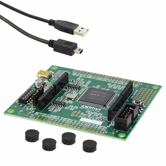
The 10M08SAE144C8G is widely used in industrial control, motor drives, sensor hubs, LED display controllers, and IoT edge devices. The image below shows the MAX 10 FPGA 10M08 Evaluation Kit, which provides a reference design platform for prototyping with this device:
Typical Application Areas:
- Sensor Fusion & Data Acquisition — the integrated ADC enables direct connection of analog sensors (temperature, pressure, current) without external ADC ICs, reducing BOM cost and board area
- Motor Control — hardware PWM generation combined with ADC feedback creates a compact single-chip motor controller
- Protocol Bridge / Interface Conversion — implement SPI-to-I2C, UART-to-Ethernet, or custom serial protocol converters
- LED Panel Controller — the high I/O count and deterministic timing make it suitable for driving LED matrices and display panels
- IoT Edge Processing — Nios II soft processor combined with the ADC enables edge analytics and local decision-making
Design Tips:
- Use the single 3.3V supply configuration (SA variant) to minimize the number of power rails and simplify PCB routing
- Enable the internal oscillator for applications that do not require high clock accuracy, eliminating an external crystal
- Leverage dual-image configuration flash for over-the-air firmware updates with automatic fallback to a known-good image
- Use the Quartus Prime Lite Edition (free) Signal Tap Logic Analyzer for in-system debugging without additional hardware
Video Tutorial: Getting Started with MAX 10 FPGA
Frequently Asked Questions
What is the difference between 10M08SAE144C8G and 10M08SCE144C8G?
The "SA" in 10M08SAE144C8G indicates a single-supply analog variant with an integrated 12-bit ADC and internal voltage regulators, so only a single 3.3V supply is needed. The "SC" variant (10M08SCE144C8G) is a single-supply core-only version without the ADC block. Choose the SA variant when your design requires analog-to-digital conversion; choose SC if you only need digital logic and want a lower-cost option.
What development tools are needed to program the 10M08SAE144C8G?
You need Intel Quartus Prime Lite Edition (free download) for design entry, synthesis, and programming. A USB Blaster or USB Blaster II programmer is required for JTAG-based configuration. The Quartus Prime software includes the Nios II Embedded Design Suite for soft processor development and ModelSim-Intel FPGA for simulation.
How many analog input channels does the 10M08SAE144C8G support?
The integrated ADC supports up to 18 analog input channels (depending on the pin configuration), with a 12-bit resolution and up to 1 MSPS sampling rate. It also includes an internal temperature sensor and voltage reference. Analog inputs are accessible through dedicated ANAIN pins on the 144-EQFP package.
Can the 10M08SAE144C8G be used without an external configuration memory?
Yes. The MAX 10 FPGA has on-chip configuration flash memory that stores up to two configuration images. This eliminates the need for external configuration PROMs or SPI flash devices. The device supports instant-on operation, booting from internal flash within milliseconds of power-up, and dual-image boot enables safe remote firmware updates.
What is the maximum operating frequency of the 10M08SAE144C8G?
The 10M08SAE144C8G (C8 speed grade) supports a maximum internal clock frequency dependent on the design complexity, typically up to 300 MHz for simple register-to-register paths. The two on-chip PLLs can generate clock frequencies from approximately 5 MHz to 472.5 MHz. The actual achievable frequency depends on the logic utilization and routing congestion of your specific design.
Is the 10M08SAE144C8G suitable for production or only prototyping?
The 10M08SAE144C8G is a production-grade device with guaranteed commercial temperature range (0°C to 85°C), RoHS compliance, and long-term availability from Intel. Its low unit cost, single-supply operation, and integrated ADC make it a popular choice for volume production in industrial automation, consumer electronics, and IoT products. An industrial-grade variant (10M08SAE144I7G) is available for extended temperature applications (-40°C to 100°C).


