
10M16SAU169C8G Datasheet, Pinout, Block Diagram & Application Guide | Intel MAX 10 FPGA
The 10M16SAU169C8G is a non-volatile, single-chip FPGA from Intel's (formerly Altera) MAX 10 family, fabricated on TSMC's 55 nm flash process. It integrates 16,000 logic elements, 562 Kbit of M9K embedded SRAM, 45 hardware 18×18-bit multipliers, dual on-die configuration flash images, user flash memory, 2 PLLs, and a 12-bit 1 MSPS SAR ADC — all within a compact 169-pin UFBGA package. Operating from a single 3.3 V supply with instant-on boot (under 10 ms), the 10M16SAU169C8G eliminates external configuration memory, reducing BOM cost and board area for industrial control, communications, IoT edge, and mixed-signal applications.
Overview and Part Number Decoding
The 10M16SAU169C8G belongs to the Intel MAX 10 product line — the industry's first single-chip, non-volatile FPGA family. Unlike SRAM-based FPGAs such as Xilinx Spartan-7 or Intel Cyclone V that require external SPI flash for configuration bitstream storage, MAX 10 devices store up to two complete configuration images in on-die flash memory. This architecture enables instant-on operation within milliseconds of power-up and supports fail-safe remote field updates via the Remote System Upgrade (RSU) IP core — without any external EPCQ or SPI NOR flash on the BOM.
A key differentiator of the “SA” variant is the integrated 12-bit, 1 MSPS SAR ADC with up to 9 external analog input channels and an internal temperature sensor. This on-chip ADC eliminates the need for an external ADC IC, saving board space, reducing BOM cost, and simplifying routing in mixed-signal designs such as sensor acquisition, power monitoring, and industrial control.
The part number encodes the following attributes:
- 10M16 — MAX 10 family, 16,000 logic elements
- SA — Single-supply, Analog variant (internal 1.2 V regulator + integrated 12-bit ADC)
- U169 — 169-ball Ultra FineLine BGA (UFBGA, 11 × 11 mm body, 0.8 mm pitch)
- C8 — Commercial temperature range (0 °C to +85 °C), speed grade 8
- G — Green / RoHS / Pb-free compliant
The “SA” designation distinguishes this variant from the “SC” (single-supply, compact) variants that omit the analog-to-digital converter. In the SC variant, the analog input pins become general-purpose digital I/O or LVDS channels instead. The device is fully supported by Intel Quartus Prime Lite Edition, which is free to download and requires no license file. For current stock and pricing, check 10M16SAU169C8G availability on WWDParts.
Specifications and Parameter Table
| Parameter | Value |
|---|---|
| Manufacturer | Intel (Altera) |
| Product Family | MAX 10 |
| Part Number | 10M16SAU169C8G |
| Logic Elements (LEs) | 16,000 |
| Logic Array Blocks (LABs) | 1,000 (16 LEs per LAB) |
| M9K Embedded Memory Blocks | 61 |
| Total Embedded SRAM | 562 Kbit (562,176 bits) |
| 18×18 Embedded Multipliers | 45 |
| Phase-Locked Loops (PLLs) | 2 (4 output counters each) |
| User Flash Memory (UFM) | 2,876 Kbit |
| Configuration Flash Memory | Dual-image internal flash (instant-on, <10 ms boot) |
| Integrated ADC | 1 × 12-bit SAR ADC, 1 MSPS, up to 9 analog channels + temperature sensor |
| User I/O Pins (U169 package) | 130 |
| I/O Banks | 8 |
| Global Clock Networks | 20 |
| Maximum LVDS Differential Pairs | 36 |
| I/O Standards Supported | 3.3 V / 2.5 V / 1.8 V / 1.5 V LVTTL/LVCMOS, LVDS, SSTL, HSTL |
| Maximum Fabric Frequency | 402 MHz (register-to-register, speed grade 8) |
| M9K Maximum Speed | 284 MHz |
| Core Voltage (VCC) | 1.2 V (internally regulated from 3.3 V) |
| External Supply (VCCA / VCCIO) | 3.3 V single rail (2.85–3.465 V) |
| Process Node | 55 nm (TSMC flash process) |
| Package | 169-UFBGA (11 × 11 mm, 0.8 mm pitch) |
| Operating Temperature (TJ) | 0 °C to +85 °C (Commercial) |
| Moisture Sensitivity Level | MSL 3 |
| RoHS / Pb-Free | Yes |
The 10M16SAU169C8G doubles the logic capacity of the 10M08SAE144C8G while maintaining the same single-supply architecture. With 45 embedded 18×18 multipliers, the device can efficiently implement DSP functions, FIR filters, and fixed-point arithmetic without consuming logic element resources.
Architecture and Block Diagram
The MAX 10 architecture integrates logic array blocks (LABs), M9K memory blocks, 18×18 multiplier-accumulator (MAC) blocks, PLLs, configuration flash, user flash memory (UFM), and a 12-bit ADC on a single die. Each LAB contains 16 adaptive logic modules (ALMs) that can be configured as combinational functions, registers, or both. The M9K blocks support true dual-port, simple dual-port, and single-port modes with independently configurable widths from ×1 to ×36.

The dual configuration flash images allow over-the-air (OTA) firmware updates with rollback protection. If a new image fails CRC verification during boot, the device automatically reverts to the factory “golden” image, ensuring uninterrupted operation. The 2,876 Kbit UFM block provides non-volatile storage for calibration tables, serial numbers, encryption keys, or boot parameters without any external EEPROM.
The two on-chip PLLs each provide four independent output clocks with frequency synthesis up to 472.5 MHz, supporting phase shifts in 45° increments and dynamic reconfiguration at runtime. The PLLs accept input frequencies from 5 MHz to 472.5 MHz and can multiply or divide to generate the required domain clocks for multi-clock designs.
Pinout, Package, and PCB Layout
The 10M16SAU169C8G uses a 169-ball UFBGA package with a 13 × 13 ball grid in an 11 × 11 mm body. The 0.8 mm ball pitch permits routing on standard 4-layer PCBs with 4/4 mil trace/space design rules. The compact form factor is well-suited for space-constrained embedded designs.

Key PCB layout recommendations for the 10M16SAU169C8G:
- Power planes — Dedicate a full inner layer to 3.3 V supply with a separate ground plane. Place 100 nF MLCC decoupling capacitors on every VCC and VCCIO ball, as close to the BGA pads as possible.
- ADC routing — Keep analog input traces short and isolated from digital signals. Use guard traces tied to AGND around each analog channel to minimize crosstile noise coupling.
- JTAG access — Bring TCK, TMS, TDI, TDO, and TRST to a standard 10-pin JTAG header for programming and in-system debugging via the Intel USB-Blaster II.
- Thermal management — The exposed thermal pad on the bottom of the UFBGA must be soldered to a copper pour connected to the ground plane through an array of thermal vias for proper heat dissipation.
For the complete pin assignment file and I/O bank voltage assignments, refer to the official 10M16SAU169C8G product page on WWDParts.
Application Circuits and Design Guidelines
The 10M16SAU169C8G is an ideal fit for applications requiring a compact, non-volatile FPGA with mixed-signal capabilities. Common deployment scenarios include:
- Industrial sensor hubs — The on-chip ADC samples up to 9 analog channels (temperature, pressure, current) while the logic fabric implements SPI/I²C aggregation, Modbus RTU framing, and threshold alerting — all in a single 11 × 11 mm package.
- Motor control — With 45 embedded multipliers, the device supports real-time FOC (Field Oriented Control) algorithms with space-vector PWM output, position encoder interface (QEP/SinCos), and over-current protection logic.
- Communication protocol bridging — Implement UART-to-Ethernet, PCIe-to-SPI, or CAN-to-RS-485 protocol bridges with hardware-level deterministic latency, replacing software-based solutions that consume CPU cycles.
- LED/display controllers — Drive large LED panels, seven-segment multiplexed displays, or TFT interfaces with built-in frame buffers stored in M9K blocks.
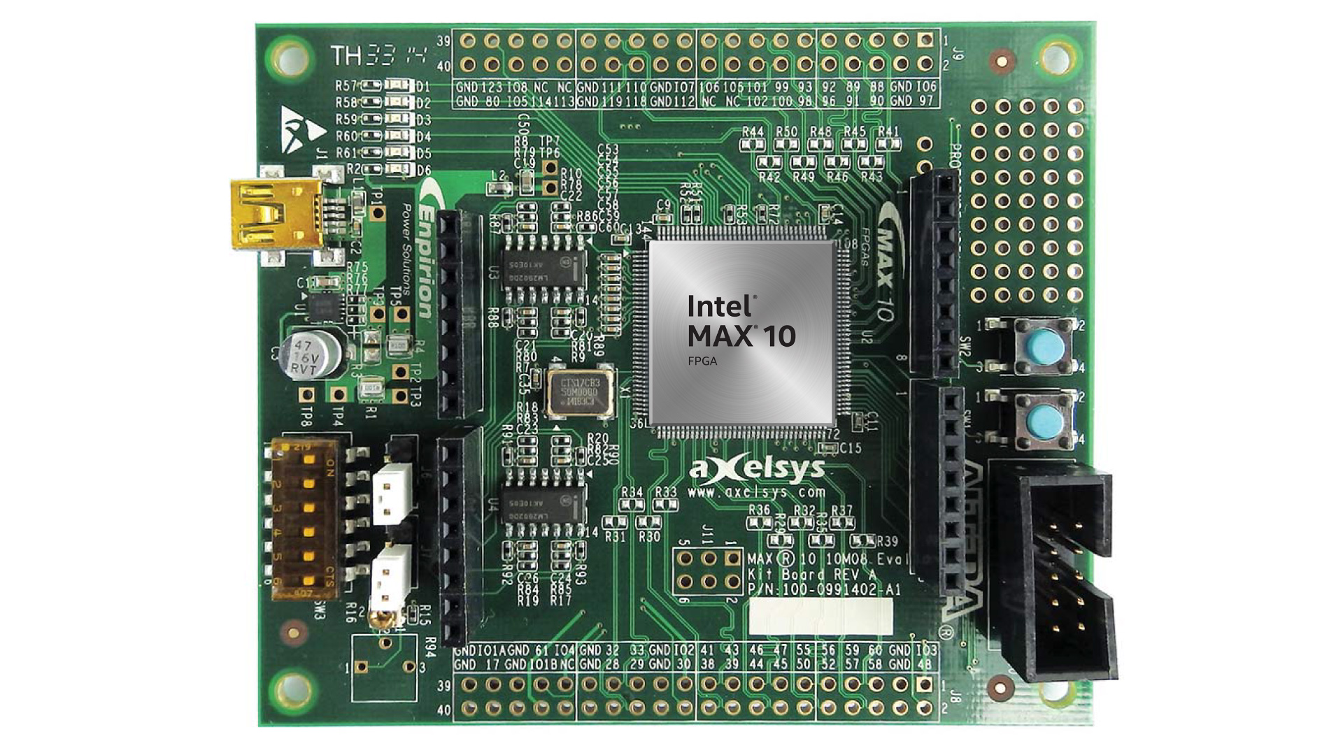
A minimal application circuit for the 10M16SAU169C8G requires only the 3.3 V supply rail, decoupling capacitors, JTAG programming header, and optional 50 MHz oscillator. The internal voltage regulator generates the 1.2 V core supply, eliminating a separate switching regulator from the BOM. For detailed schematic examples and reference designs, Intel provides the MAX 10 FPGA Evaluation Kit hardware reference design as a starting point.
Frequently Asked Questions (FAQ)
1. What is the difference between 10M16SAU169C8G and 10M16SCU169C8G?
Both share the same 16,000 LE fabric in a 169-UFBGA package. The “SA” variant (10M16SAU169C8G) includes an integrated 12-bit SAR ADC with up to 9 external analog input channels, whereas the “SC” variant omits the ADC, and those pins become general-purpose digital I/O or LVDS channels. Choose the SA variant when your design needs on-chip analog-to-digital conversion; otherwise the SC variant provides additional digital I/O.
2. Does the 10M16SAU169C8G require an external configuration flash?
No. MAX 10 devices store configuration bitstreams in internal flash memory, supporting up to two images for instant-on boot and fail-safe remote updates. This eliminates the EPCQ, SPI NOR, or QSPI flash typically required by SRAM-based FPGAs and reduces BOM cost and board area.
3. What development software is required for the 10M16SAU169C8G?
The device is fully supported by Intel Quartus Prime Lite Edition, which is free to download with no license file required. Quartus Prime Lite includes the full synthesis, place-and-route, timing analysis, and programming tool chain. For simulation, ModelSim – Intel FPGA Starter Edition is bundled at no cost.
4. Can the 10M16SAU169C8G support LVDS high-speed interfaces?
Yes. The U169 package supports up to 36 LVDS differential pairs operating at up to 875 Mbps data rate per pair. LVDS I/O is available on dedicated I/O banks and supports both LVDS transmit and receive with on-chip differential termination resistors.
5. What is the maximum operating frequency of the 10M16SAU169C8G?
Speed grade 8 (the C8 suffix) achieves up to 402 MHz register-to-register fabric performance and 284 MHz M9K memory speed. The PLLs support output frequencies up to 472.5 MHz. Actual design performance depends on utilization, routing congestion, and timing constraints.
6. Is the 10M16SAU169C8G suitable for automotive or military applications?
The C8G suffix designates commercial temperature range (0 °C to +85 °C). For extended industrial temperature (–40 °C to +100 °C), select the 10M16SAU169I7G variant. MAX 10 devices are not currently offered in military (MIL-STD-883) or automotive (AEC-Q100) qualified grades.


