
10M16SAU169I7G Datasheet, Specifications & Pinout – Altera MAX 10 FPGA Guide
1. 10M16SAU169I7G Overview
The 10M16SAU169I7G is a non-volatile FPGA from the Intel (Altera) MAX 10 family, built on a 55 nm flash process technology. Part of the MAX 10 series, this device combines FPGA flexibility with instant-on capability thanks to its integrated configuration flash memory — eliminating the need for an external configuration device. It features 16,000 logic elements (LEs), up to 549 Kb of embedded SRAM, an integrated analog-to-digital converter (ADC), and 4 PLLs, all housed in a compact 169-pin UBGA package. The "I7G" suffix indicates an industrial temperature grade (-40°C to +100°C) with speed grade 7, making it ideal for harsh-environment industrial, automotive, and IoT edge applications.
The MAX 10 family is designed to bridge the gap between CPLDs and FPGAs, offering single-chip, non-volatile programmable logic with features previously only available in more expensive device families. The 10M16SAU169I7G is widely used in motor control, sensor hubs, I/O expansion, protocol bridging, and embedded display applications. You can find this part available at trusted distributors such as wwdparts.com.
2. Key Specifications & Parameters
| Parameter | Value |
|---|---|
| Manufacturer | Intel (Altera) |
| Family | MAX 10 FPGA |
| Part Number | 10M16SAU169I7G |
| Logic Elements (LEs) | 16,000 |
| Logic Array Blocks (LABs) | 1,000 |
| Embedded Memory (SRAM) | 549 Kb (562,176 bits) |
| User Flash Memory | Built-in (UFM) |
| Phase-Locked Loops (PLLs) | 4 |
| 18×18 Embedded Multipliers | 45 |
| Analog-to-Digital Converter (ADC) | Yes (dual 12-bit, 1 MSPS) |
| Maximum User I/O Pins | 130 (U169 package) |
| Maximum LVDS Pairs | 22 |
| I/O Standards | 3.3V / 2.5V / 1.8V / 1.5V LVCMOS, LVTTL, SSTL, HSTL, LVDS |
| External Memory Interface | DDR2, DDR3, LPDDR2, SRAM |
| Core Voltage | 1.2 V |
| I/O Supply Voltage | 1.0 V – 3.3 V |
| Process Technology | 55 nm Flash |
| Package | UBGA-169 (11 mm × 11 mm) |
| Mounting Type | SMD / SMT (BGA) |
| Operating Temperature | -40°C to +100°C (Industrial) |
| Speed Grade | 7 |
| Configuration | Internal (no external config device needed) |
| Bitstream Security | AES 128-bit encryption |
3. Block Diagram & Architecture
The MAX 10 FPGA architecture integrates logic elements, embedded memory blocks, DSP blocks with 18×18 multipliers, an ADC block, and user flash memory into a single die. The block diagram below illustrates the internal architecture of the MAX 10 family, showing the arrangement of logic array blocks (LABs), M9K memory blocks, PLLs, I/O elements, and the integrated ADC. This single-chip architecture eliminates the need for external configuration flash, reducing board space and BOM cost.

The MAX 10 architecture supports dual configuration images for remote system update, enabling fail-safe in-field firmware upgrades — a critical feature for deployed IoT and industrial systems. For detailed signal descriptions, refer to the Altera FPGA collection on wwdparts.com.
4. Pinout & Package Information
The 10M16SAU169I7G uses the UBGA-169 (Ultra Fine-Pitch Ball Grid Array) package with 169 solder balls arranged in a 13×13 grid with 0.8 mm pitch. The compact 11 mm × 11 mm body size makes it suitable for space-constrained designs. Up to 130 user I/O pins are available, organized into multiple I/O banks supporting a range of voltage standards from 1.0 V to 3.3 V. The device supports LVDS differential signaling on select pin pairs for high-speed data transfer.

Key pin categories include dedicated clock inputs (CLK), JTAG programming pins (TCK, TMS, TDI, TDO), power supply pins (VCC, VCCIO), and analog input pins for the integrated ADC. When designing a PCB layout, ensure proper power plane separation between VCC (1.2V core) and VCCIO (bank-specific I/O voltage) rails. Decoupling capacitors should be placed as close to the BGA pads as possible.
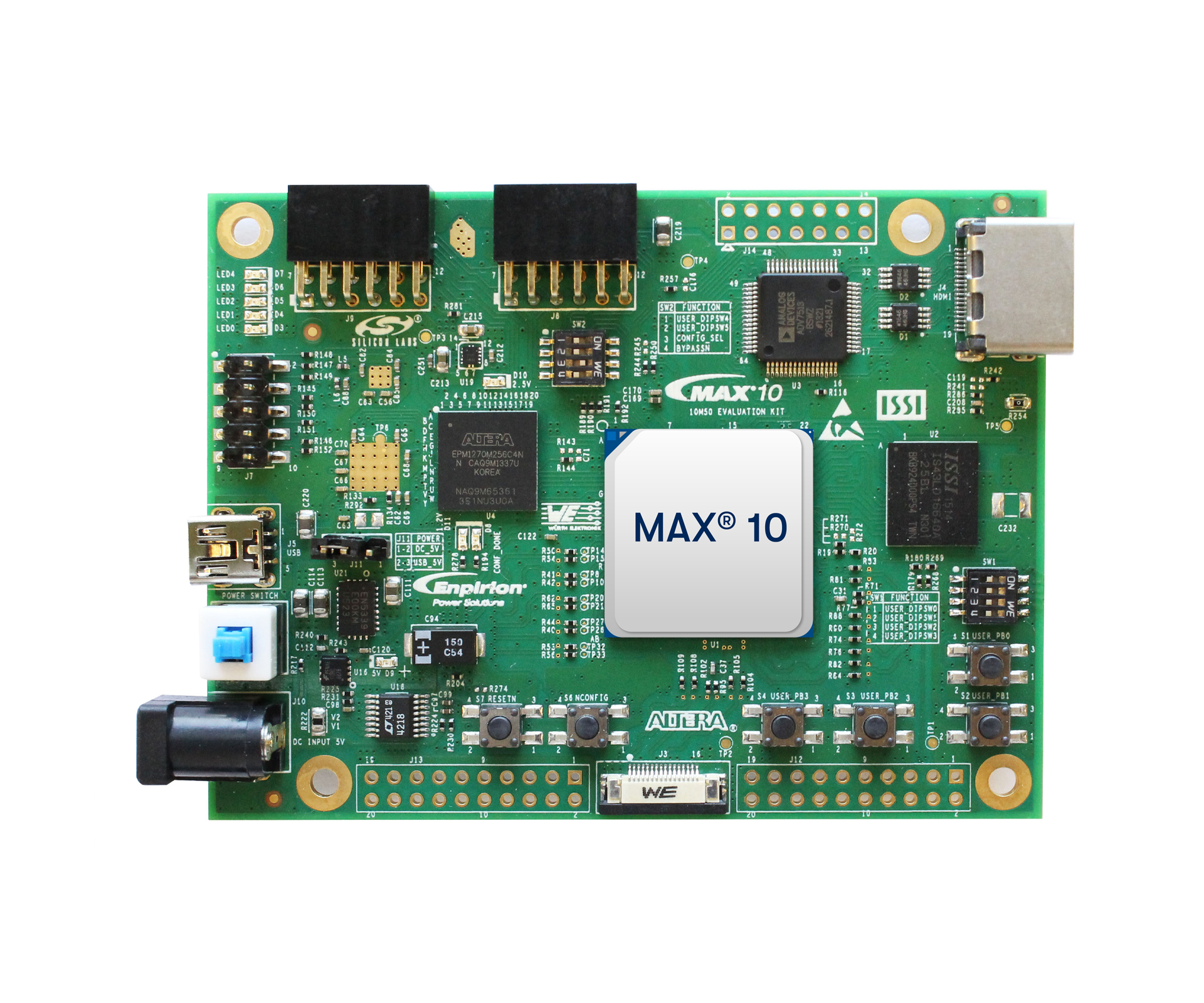
5. Application Circuit & Development Kit
The MAX 10 FPGA is commonly used in a wide range of embedded applications including sensor aggregation, motor control, protocol bridging (SPI/I2C/UART to parallel), display control, and as a co-processor alongside MCUs or SoCs. Below is the MAX 10 FPGA Evaluation Kit, which provides a ready-to-use hardware platform for prototyping and evaluating the MAX 10 device family.
A typical application circuit for the 10M16SAU169I7G includes: (1) a 3.3V and 1.2V power supply using LDO or switching regulators, (2) bypass capacitors on every VCC and VCCIO pin, (3) a JTAG header for programming via USB Blaster, (4) a 50 MHz oscillator connected to a dedicated clock input, and (5) configuration mode pins (MSEL) tied to select internal configuration mode. Intel's Quartus Prime Lite Edition (free) provides the complete design flow from RTL to bitstream for the MAX 10 family. Explore compatible components and development tools at wwdparts.com FPGA collection.
Video Tutorial: Getting Started with MAX 10 FPGA
6. Frequently Asked Questions (FAQ)
Q1: What is the 10M16SAU169I7G?
The 10M16SAU169I7G is a non-volatile FPGA from Intel's (Altera's) MAX 10 family. It contains 16,000 logic elements, 549 Kb of embedded SRAM, an integrated 12-bit ADC, 4 PLLs, and 45 embedded multipliers in a 169-pin UBGA package. It operates at industrial temperature range (-40°C to +100°C) with speed grade 7.
Q2: Does the 10M16SAU169I7G require an external configuration flash?
No. The MAX 10 FPGA family features integrated configuration flash memory, allowing single-chip instant-on operation without any external configuration device. This reduces BOM cost and board space while enabling dual-image configuration for fail-safe remote updates.
Q3: What software tools are needed to program the 10M16SAU169I7G?
Intel Quartus Prime Lite Edition (free) fully supports the MAX 10 FPGA family. It provides a complete design flow including RTL entry (Verilog/VHDL), synthesis, place-and-route, timing analysis, and bitstream generation. Programming is done via a USB Blaster or USB Blaster II through the JTAG interface.
Q4: What are the power supply requirements for the 10M16SAU169I7G?
The device requires a 1.2V core supply (VCC) and I/O bank supplies (VCCIO) ranging from 1.0V to 3.3V depending on the I/O standard used. A separate analog supply (VCCADC) is needed when using the integrated ADC. Each supply rail requires proper decoupling with both bulk and high-frequency bypass capacitors.
Q5: What is the difference between speed grades in MAX 10 FPGAs?
Speed grade indicates the performance tier of the device. The 10M16SAU169I7G has speed grade 7 (the "7" in I7G). Lower numbers indicate faster devices. Speed grade affects maximum clock frequencies, setup/hold times, and propagation delays. For the highest performance in timing-critical designs, select a lower speed grade number.
Q6: Can the 10M16SAU169I7G interface with DDR3 memory?
Yes. The MAX 10 FPGA supports DDR3 SDRAM, DDR2 SDRAM, LPDDR2, and standard SRAM external memory interfaces. The hard memory controller IP available through Quartus Prime simplifies the implementation of high-speed memory interfaces. Note that the number of available memory interface pins depends on the specific package variant.


