
The 10M16SAU169I7G is an industrial-grade, non-volatile FPGA from the Intel (Altera) MAX 10 family. Built on a 55 nm flash process, it delivers 16,000 logic elements, an integrated dual 12-bit ADC, and instant-on configuration — all in a compact 169-ball UBGA package rated for the full −40 °C to +100 °C industrial temperature range. This guide covers its key specifications, block diagram, pinout, typical application circuits, and answers to frequently asked questions.
Table of Contents
- 1. Key Specifications & Parameters
- 2. Block Diagram
- 3. Pinout & Package Information
- 4. Typical Application Circuit
- 5. Equivalents & Cross-Reference
- 6. Frequently Asked Questions
1. Key Specifications & Parameters
The table below summarises the critical electrical, thermal, and logic parameters of the 10M16SAU169I7G extracted from the official MAX 10 datasheet.
| Parameter | Value |
|---|---|
| Part Number | 10M16SAU169I7G |
| Family / Series | Intel (Altera) MAX 10 |
| Logic Elements (LEs) | 16,000 |
| Logic Array Blocks (LABs) | 1,000 |
| M9K Memory Blocks | 66 (549 Kbit) |
| Total RAM Bits | 562,176 |
| Embedded Multipliers (18 × 18) | 45 |
| PLLs | 4 |
| Analog-to-Digital Converter | Dual 12-bit, 1 MSPS (up to 18 channels) |
| User Flash Memory (UFM) | 2,304 Kbit |
| Maximum User I/O | 130 |
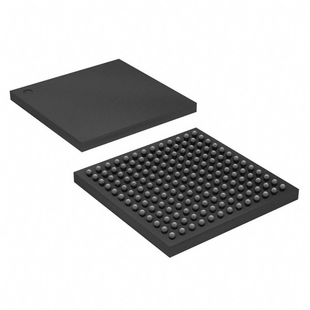
| Package | 169-ball UBGA (11 × 11 mm) |
| Core Voltage (VCCINT) | 1.2 V |
| I/O Voltage (VCCIO) | 1.2 / 1.5 / 1.8 / 2.5 / 3.0 / 3.3 V |
| Speed Grade | 7 (lowest power) |
| Operating Temperature | −40 °C to +100 °C (Industrial) |
| Process Technology | 55 nm Flash |
| Configuration | Internal (single-image / dual-image boot) |
| Mounting | SMD / SMT (Pb-free, RoHS compliant) |
For full electrical characteristics, switching times, and power estimation, refer to the Intel MAX 10 Device Handbook (PDF).
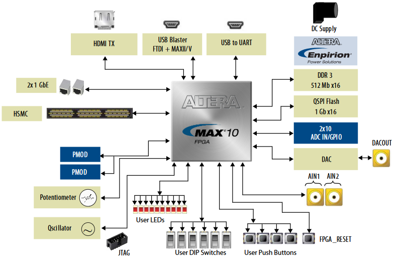
2. Block Diagram
The MAX 10 architecture integrates logic, memory, DSP, clocking, ADC, and flash configuration into a single monolithic die. The block diagram below highlights the major functional units available in the 10M16SAU169I7G.
Key architectural features include:
- Logic Array Blocks (LABs): 1,000 LABs, each containing 16 adaptive logic modules (ALMs) / logic elements for fine-grained combinational and sequential logic.
- M9K Embedded Memory: 66 blocks of 9-Kbit dual-port SRAM, configurable as ROM, single-port RAM, or FIFO buffers.
- 18 × 18 Multipliers: 45 hardware multipliers for DSP-intensive applications such as digital filtering and motor control.
- Integrated ADC: Dual 12-bit SAR ADC with up to 1 MSPS throughput, reducing external component count.
- Internal Flash Configuration: Supports single-image and dual-image boot for instant-on and remote update capabilities.
3. Pinout & Package Information
The 10M16SAU169I7G ships in a 169-ball UBGA package measuring 11 × 11 × 1.55 mm. The compact BGA footprint supports up to 130 user I/O pins across multiple I/O banks, each independently configurable for different voltage standards.
Pin assignment highlights:
- I/O Banks: Multiple I/O banks support single-ended standards (LVCMOS, LVTTL) and differential standards (LVDS) for flexible board design.
- Dedicated Pins: JTAG (TCK, TMS, TDI, TDO), configuration (nCONFIG, nSTATUS, CONF_DONE), and power/ground.
- ADC Input Pins: Dedicated analog input pins routed to the on-chip dual 12-bit ADC — no external ADC IC required.
- Clock Inputs: Dedicated global clock pins feed the four on-chip PLLs for jitter-cleaned, frequency-synthesised clocking.
For the complete ball-map and recommended PCB land pattern, consult the MAX 10 FPGA Device Architecture documentation.
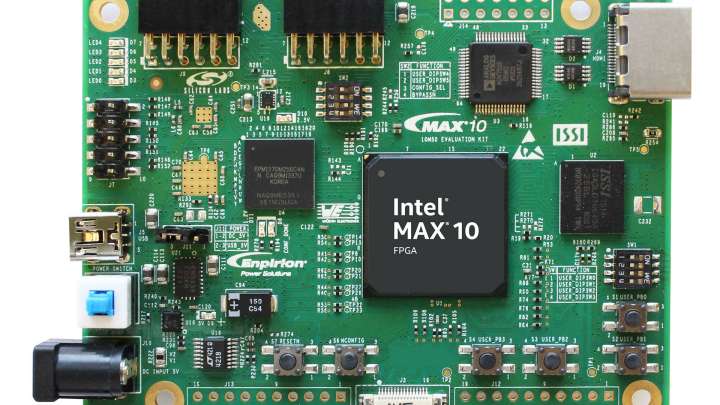
4. Typical Application Circuit
The 10M16SAU169I7G is commonly deployed on evaluation and development boards alongside DDR3 SDRAM, SPI flash, voltage regulators, and I/O level-shifters. The image below shows a representative MAX 10 FPGA development board layout.
Typical design considerations:
- Power Supply: A single 3.3 V input rail, stepped down to 1.2 V core via an integrated or external DC-DC converter, simplifies the BOM.
- Decoupling: Place 100 nF MLCC capacitors on every VCC ball and bulk 10 μF capacitors near the package perimeter.
- Configuration: Internal configuration flash eliminates the need for an external serial PROM, enabling instant-on operation within milliseconds of power-up.
- ADC Front-End: For best ADC performance, add a low-pass RC anti-alias filter (e.g., 100 Ω + 100 pF) on each analog input channel.
5. Equivalents & Cross-Reference
Engineers evaluating the 10M16SAU169I7G may also consider these related parts within the MAX 10 family and broader Intel FPGA portfolio:
| Part Number | Difference vs. 10M16SAU169I7G |
|---|---|
| 10M16SAU169C8G | Same die, commercial temp (0–85 °C), speed grade 8 |
| 10M08SAE144C8G | 8K LEs, 144-EQFP package, commercial temp |
| 10M04SCE144C8G | 4K LEs, 144-EQFP package, commercial temp |
Browse all available MAX 10 FPGA parts on wwdparts.com.
Video: Getting Started with MAX 10 FPGAs
6. Frequently Asked Questions
Q1: What is the difference between the 10M16SAU169I7G and the 10M16SAU169C8G?
The "I7G" variant is rated for the extended industrial temperature range (−40 °C to +100 °C) at speed grade 7, while the "C8G" is a commercial-temperature device (0 °C to +85 °C) at speed grade 8. The silicon die is identical; the difference lies in tested operating conditions and guaranteed timing margins.
Q2: Does the 10M16SAU169I7G require an external configuration memory?
No. The MAX 10 family integrates on-chip flash configuration memory that supports both single-image and dual-image boot. The device configures itself internally within milliseconds of power-up, eliminating the need for external serial configuration PROMs.
Q3: How many analog input channels does the integrated ADC support?
The 10M16SAU169I7G contains a dual 12-bit ADC block capable of sampling up to 1 MSPS. Depending on the pinout and I/O bank assignment, up to 18 analog channels can be routed to the ADC, including a dedicated internal temperature-sensing diode channel.
Q4: What development tools are needed to program the 10M16SAU169I7G?
Intel Quartus Prime Lite Edition (free) fully supports MAX 10 devices. Design entry is via Verilog, VHDL, or schematic capture. Programming is done through the JTAG interface using an Intel USB-Blaster or compatible programmer.
Q5: Can the 10M16SAU169I7G interface with DDR3 memory?
Yes. The MAX 10 family supports external memory interfaces including DDR3 at up to 300 MHz (600 Mbps). The device provides dedicated hard memory controller blocks and calibrated I/O to interface with standard DDR3 and DDR3L SDRAM components.
Q6: Is the 10M16SAU169I7G suitable for safety-critical or automotive applications?
The industrial-grade temperature rating (−40 °C to +100 °C) makes it suitable for harsh-environment industrial applications. For automotive-grade requirements (AEC-Q100), check Intel's automotive-qualified MAX 10 variants. The device supports SEU mitigation and on-chip CRC error detection for enhanced reliability.


