
10M04SCE144C8G Datasheet, Pinout, Equivalents, and Specs
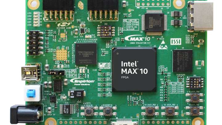
The 10M04SCE144C8G is a non-volatile FPGA from Intel's (formerly Altera) MAX 10 family, fabricated on a 55nm flash process. With 4,000 logic elements, 189 Kb of embedded SRAM, 16 embedded 18×18 multipliers, 2 PLLs, and an integrated 12-bit ADC block, it targets cost-sensitive and space-constrained designs that demand instant-on operation without external configuration memory. The device ships in a 144-pin EQFP package (20 × 20 mm) at commercial temperature grade (0 °C to 85 °C) with a C8 speed grade and single-supply 1.2 V core operation.
What Is the 10M04SCE144C8G?
The 10M04SCE144C8G belongs to the MAX 10 FPGA family — Intel's lowest-cost, single-chip programmable logic platform with integrated flash configuration storage. The "SC" in the part number designates the single-supply compact variant, meaning the device operates from a single 1.2 V core rail while embedding one analog-to-digital converter (ADC) block. Unlike traditional FPGAs that require an external serial configuration ROM, the MAX 10 stores its bitstream in on-die flash memory, enabling true instant-on power-up in under 10 ms — critical for industrial control loops, motor drives, and sensor front-ends where boot latency is unacceptable.
Internally the device organizes 4,000 logic elements (LEs) into 250 logic array blocks (LABs), each containing 16 LEs with a 4-input look-up table (LUT) and a programmable register. Embedded memory is distributed across 21 M9K blocks (each providing 9,216 bits of true dual-port SRAM), totaling 189 Kb of on-chip storage configurable as single-port RAM, dual-port RAM, shift registers, FIFO buffers, or ROM. For DSP workloads, 16 embedded 18×18 multiplier blocks support signed/unsigned integer multiplication with optional accumulation, enabling efficient implementation of FIR filters and control-loop math at up to 284 MHz internal clock speeds.
Pinout Configuration and Packaging
The 10M04SCE144C8G is housed in a 144-pin Enhanced Quad Flat Pack (EQFP) package designated E144, measuring 20 × 20 mm with a 0.5 mm lead pitch and an exposed thermal pad on the underside. Of the 144 pins, 101 are available as general-purpose user I/O distributed across 8 I/O banks. Each I/O bank supports independent VCCIO supply rails, enabling mixed-voltage interfacing at 1.2 V, 1.5 V, 1.8 V, 2.5 V, and 3.3 V within a single device. The I/O structure supports LVTTL, LVCMOS, PCI, SSTL, HSTL, HSUL, and LVDS standards, with up to 15 differential LVDS pairs available in this package variant.
Critical power pins include VCC (1.2 V core supply), VCCIO (per-bank selectable), and VCCA (1.2 V analog PLL/ADC supply). The integrated ADC block provides 1 dedicated analog input pin and 8 dual-function pins that can serve as either digital I/O or analog-to-digital converter inputs, offering up to 12-bit resolution at 1 MSPS. Configuration is handled entirely from internal flash — no MSEL strapping is required for the single-image boot mode, though dual-image support allows storing 2 compressed configuration images for remote update with automatic fallback. JTAG boundary-scan is supported for in-system programming and debug via the standard TCK, TDI, TDO, and TMS pins.

Specifications Parameter Table
| Specification | Technical Details |
|---|---|
| Device Family | MAX 10 (Intel / Altera) |
| Logic Elements (LEs) | 4,000 |
| Logic Array Blocks (LABs) | 250 |
| Embedded Memory (M9K) | 189 Kb (21 M9K blocks × 9 Kb) |
| 18×18 Multipliers | 16 |
| PLLs | 2 |
| ADC Blocks | 1 (12-bit, up to 1 MSPS, 9 channels) |
| User I/O (E144) | 101 |
| LVDS Pairs (E144) | Up to 15 |
| User Flash Memory (UFM) | 64 Kb |
| Configuration Flash | Internal (dual-image, 2 compressed images) |
| I/O Standards | 3.3 V / 2.5 V / 1.8 V / 1.5 V / 1.2 V LVCMOS, LVTTL, PCI, SSTL, HSTL, LVDS |
| Core Supply (VCC) | 1.2 V (single supply) |
| I/O Supply (VCCIO) | 1.2 V to 3.3 V (per-bank) |
| Temperature Range | 0 °C to 85 °C (Commercial) |
| Speed Grade | C8 |
| Process Technology | 55 nm flash |
| Package | 144-EQFP (E144), 20 × 20 mm, 0.5 mm pitch |
| RoHS Compliance | Yes (Lead-free) |
| Status | Active / Production |
Typical Applications and Circuit Considerations
The 10M04SCE144C8G is widely deployed in industrial automation, motor-drive control, sensor-hub aggregation, and low-cost embedded processing. Its instant-on capability makes it a natural fit for safety-critical state machines that must assert control outputs within milliseconds of power application — a requirement in servo drives, power supply sequencers, and fail-safe interlock controllers. The integrated 12-bit ADC eliminates the need for an external converter in applications such as temperature monitoring, current sensing via shunt resistors, and battery management front-ends, reducing BOM cost and PCB area.
For designs requiring a soft-core processor, the MAX 10 supports the Nios II/e economy core, which fits comfortably within 4,000 LEs alongside peripheral logic. Combined with the 189 Kb of embedded SRAM and 64 Kb of user flash memory (UFM) for non-volatile data storage, the device can host small firmware images for protocol conversion, LED-panel driving, or sensor-to-SPI/I2C bridge functions. The dual-image configuration flash enables secure remote firmware updates — the active image runs while the factory fallback image remains protected, minimizing bricking risk during over-the-air upgrades. External memory interfacing is limited to SRAM in this device density, but the 101 user I/O pins provide ample connectivity for parallel buses, SPI, I2C, UART, and custom interfaces.

On the power supply side, the single-supply architecture simplifies the board design considerably. A single 1.2 V regulator feeds the core, while VCCIO banks can share the same rail or use separate supplies for multi-voltage I/O interfacing. Decoupling follows standard FPGA practice: 100 nF MLCC capacitors on every VCC/VCCIO pin with bulk 10 µF capacitors at each supply entry point. The exposed pad must be soldered to a ground plane for both thermal and electrical integrity — thermal resistance (θJA) is approximately 24 °C/W, adequate for the device's typical 300 mW core power consumption at moderate utilization.
Equivalents, Cross-Reference, and Lifecycle
Within the MAX 10 family, the closest variants to the 10M04SCE144C8G include the 10M04SAE144C8G (dual-supply analog variant with 2 ADC blocks and separate VCCIO/VCC rails), the 10M04SCE144I7G (industrial temperature −40 °C to 100 °C, I7 speed grade), and the 10M04DCE144C8G (compact variant without ADC). For designs needing more logic density in the same E144 footprint, the 10M08SAE144C8G doubles the LEs to 8,000 while maintaining pin compatibility, and the 10M16SAU169C8G scales to 16,000 LEs in a slightly larger U169 package.
From a cross-vendor perspective, Lattice Semiconductor's MachXO3LF-4300 offers similar logic density (4,300 LUTs) with integrated flash in a QFP package, though it lacks an integrated ADC. Microchip (formerly Microsemi) PolarFire and IGLOO2 devices occupy a higher tier but share the flash-based instant-on paradigm. The MAX 10 10M04 remains in active production with no end-of-life notice as of 2026, and Intel has committed to long-term supply for industrial and automotive customers through the Altera brand. For procurement flexibility, authorized distributors including wwdparts.com Intel FPGA catalog stock the 10M04SCE144C8G with full traceability.
Video Tutorial: Getting Started with MAX 10 FPGA
Frequently Asked Questions (FAQ)
1. Does the 10M04SCE144C8G require an external configuration memory chip?
No. The MAX 10 family stores its configuration bitstream in on-die flash memory, eliminating the need for an external EEPROM or serial flash. The 10M04SCE144C8G supports dual-image storage — two compressed configuration images reside internally, enabling remote update with automatic fallback to a known-good factory image if the primary image fails CRC verification during boot.
2. What is the difference between the 10M04SCE144C8G and 10M04SAE144C8G?
The "SC" suffix denotes the single-supply compact variant — the device core and I/O share a simplified power architecture with one 1.2 V core rail and features 1 ADC block. The "SA" (single analog) variant provides 2 ADC blocks with a dual-supply power architecture requiring separate core and analog supply rails. Both share identical logic resources (4,000 LEs, 189 Kb memory, 16 multipliers) and are pin-compatible in the E144 package, so the choice depends on whether you need one or two independent ADC channels and your power supply complexity budget.
3. Can I run a Nios II soft processor on the 10M04SCE144C8G?
Yes. The Nios II/e (economy) core requires approximately 600–700 LEs, leaving roughly 3,300 LEs for peripheral logic, custom accelerators, and I/O control. The 189 Kb of M9K SRAM can serve as tightly-coupled instruction and data memory, and the 64 Kb UFM provides non-volatile storage for calibration data or small firmware parameters. For applications that need more code space, an external SPI flash or SRAM connected via the 101 user I/O pins can extend the memory map.
4. What is the power consumption of the 10M04SCE144C8G?
Typical core dynamic power at moderate utilization (50% LE usage, 100 MHz clock) is approximately 150–300 mW, with standby current under 50 mA. Total system power depends heavily on I/O toggle rates, VCCIO voltage levels, and ADC activity. Intel provides the Early Power Estimator (EPE) spreadsheet and the PowerPlay Power Analyzer within Quartus Prime for accurate estimation at the design stage. The single-supply architecture reduces regulator count and associated quiescent losses compared to dual-supply variants.
5. What EDA tools and programming cables are needed?
Design entry, synthesis, place-and-route, and programming are handled by Quartus Prime Lite Edition, which is free and does not require a license file for MAX 10 devices. Programming and debug use the USB-Blaster II (or compatible clone) connected via the JTAG header (TCK, TDI, TDO, TMS, GND). In-system programming writes the .pof file directly to internal flash. The Quartus Programmer also supports .jam/.jbc files for production programming via automated test equipment (ATE).
6. What is the maximum operating frequency of the 10M04SCE144C8G?
The C8 speed grade supports internal register-to-register clock speeds of up to 284 MHz for M9K memory operations and approximately 300 MHz for logic-only paths, depending on design complexity and routing utilization. The 2 on-chip PLLs provide clock synthesis from 5 MHz to 472.5 MHz output frequency range with fine-grained phase shifting and spread-spectrum clocking for EMI reduction. Actual achievable Fmax depends on design-specific critical paths reported by the Quartus Prime Timing Analyzer after place-and-route.


