
10M04SCE144C8G Datasheet, Pinout, Specifications & Application Guide | Intel MAX 10 FPGA
The 10M04SCE144C8G is a non-volatile FPGA from Intel's (formerly Altera) MAX 10 family. Built on a 55 nm process, it integrates 4,000 logic elements, embedded SRAM, user flash memory, and a 12-bit ADC into a compact 144-pin EQFP package. With instant-on capability powered by internal configuration flash, the 10M04SCE144C8G eliminates the need for an external configuration device — making it ideal for cost-sensitive industrial, automotive, and IoT applications.
Table of Contents
- Key Specifications & Parameters
- Block Diagram & Architecture
- Pinout & Package Information
- Application Circuit & Design Guide
- Video Tutorial
- Frequently Asked Questions (FAQ)
Key Specifications & Parameters
The table below summarizes the core electrical, architectural, and physical parameters of the 10M04SCE144C8G. These values are essential for schematic design, power budgeting, and BOM selection.
| Parameter | Value |
|---|---|
| Manufacturer | Intel (Altera) |
| Family | MAX 10 (10M04) |
| Logic Elements (LEs) | 4,000 |
| Embedded Memory (M9K) | 189 Kb |
| Embedded 18×18 Multipliers | 16 |
| Phase-Locked Loops (PLLs) | 2 |
| User I/O Pins | 101 |
| Maximum LVDS Pairs | 15 |
| Analog-to-Digital Converter | 1× 12-bit SAR ADC (up to 1 MSPS) |
| User Flash Memory (UFM) | 256 Kb |
| Configuration Flash Memory (CFM) | Dual-boot capable, internal |
| Core Supply Voltage (VCC) | 1.2 V (1.15 V – 1.25 V) |
| I/O Voltage Support | 1.0 V, 1.2 V, 1.5 V, 1.8 V, 2.5 V, 3.0 V, 3.3 V |
| Process Technology | 55 nm |
| Package | 144-EQFP (20 mm × 20 mm), Exposed Pad |
| Temperature Range | –40 °C to +85 °C (Commercial) |
| Speed Grade | 8 (Standard) |
| I/O Standards | LVTTL, LVCMOS, SSTL, HSTL, HSUL, LVDS, PCI |
| Configuration Mode | Internal (instant-on), JTAG |
| RoHS Compliant | Yes (Lead-Free / Green) |
Block Diagram & Architecture
The MAX 10 architecture integrates a logic fabric with embedded memory blocks, DSP multipliers, PLLs, flash memory, and an ADC — all within a single-chip, non-volatile platform. The diagram below illustrates the evaluation kit block-level connectivity, showing how the 10M04 FPGA connects to memory interfaces, clock sources, ADC inputs, and configuration logic.
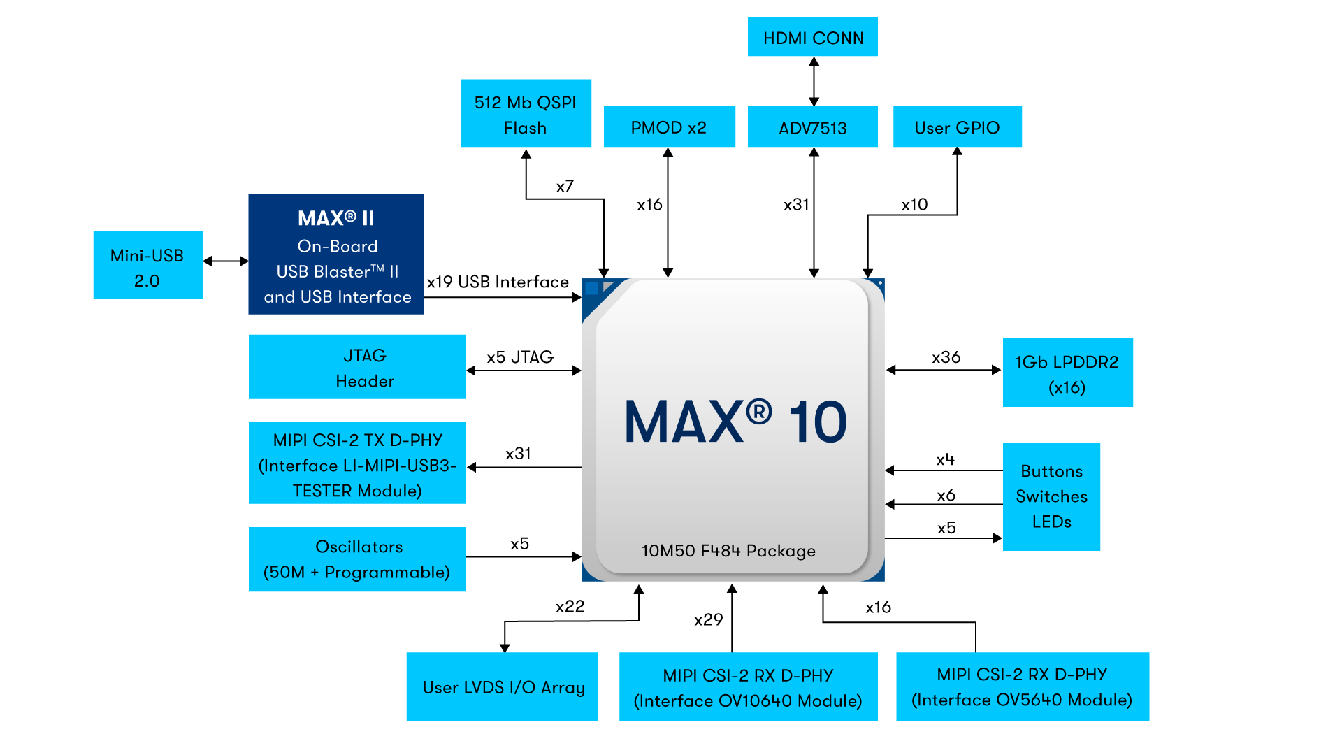
Key architectural highlights of the 10M04SCE144C8G include:
- Logic Array Blocks (LABs): Each LAB contains 16 LEs with a 4-input LUT, programmable register, and carry chain.
- M9K Memory Blocks: 9,216-bit blocks configurable as RAM, ROM, FIFO, or shift registers.
- Internal Flash: Dual configuration flash (CFM) supports instant-on and dual-boot; User Flash Memory (UFM) stores application data.
- 12-bit ADC: Up to 9 analog input channels (1 dedicated + 8 dual-function) for sensor and monitoring applications.
Pinout & Package Information
The 10M04SCE144C8G uses the 144-pin EQFP (Enhanced Quad Flat Pack) form factor measuring 20 mm × 20 mm with an exposed thermal pad. This package provides 101 user I/O pins across 8 I/O banks, supporting a wide range of voltage levels from 1.0 V to 3.3 V.

Important pin categories for the E144 package include:
- VCC / GND: Core power (1.2 V) and ground pins distributed across all four sides for low-inductance power delivery.
- VCCIO: Per-bank I/O supply pins supporting independent voltage levels on each bank.
- JTAG: TDI, TDO, TMS, TCK pins for programming and boundary-scan testing.
- Clock Inputs: Dedicated global clock input pins (CLK0–CLK3) connected to the PLL and global clock network.
- ADC Inputs: ANAIN1 (dedicated analog) plus up to 8 dual-function analog/digital pins.
- Configuration: nCONFIG, nSTATUS, CONF_DONE for device configuration control.
For the full 10M04SCE144C8G pin assignment table, refer to the Intel MAX 10 Device Handbook. You may also find our guides on similar MAX 10 devices helpful: 10M08SAE144C8G Datasheet & Pinout Guide.
Application Circuit & Design Guide
The 10M04SCE144C8G is widely deployed in industrial control, sensor fusion, motor drive, IoT gateways, and low-cost prototyping. The image below shows the Intel MAX 10 FPGA Evaluation Board — a reference design that demonstrates power supply decoupling, clock input, JTAG header, ADC analog front-end, and user I/O header connections.
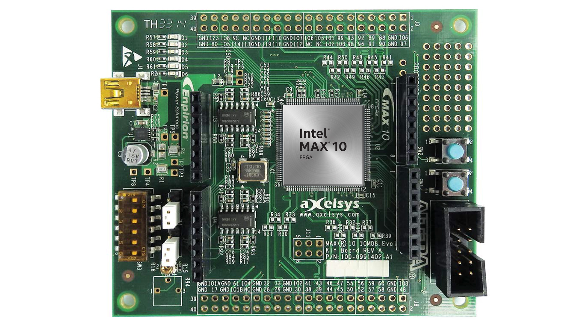
Essential design considerations for the 10M04SCE144C8G:
- Power Supply: Provide a clean 1.2 V core rail (VCC) and per-bank I/O rails (VCCIO). Use 100 nF decoupling capacitors on every power pin and a 10 µF bulk capacitor per rail.
- Clock Design: Connect an external oscillator (up to 116 MHz input) to the CLK input pins. The two on-chip PLLs can multiply and phase-shift clocks up to 500 MHz internally.
- JTAG Programming: Include a 10-pin JTAG header for Quartus Prime Programmer access via USB-Blaster.
- ADC Front-End: The 12-bit ADC accepts 0–2.5 V input range. Use a resistor-divider or op-amp scaling circuit for higher-voltage signals.
- Configuration: The MAX 10 stores its bitstream in internal flash — no external EEPROM required. Supports dual-boot images for fail-safe field updates.
For more MAX 10 design examples, see our related guides: 10M16SAU169C8G Specifications & Application Guide and 10M16SAU169I7G Datasheet & Design Guide.
Video Tutorial
Watch this hands-on tutorial to learn how to set up and program an Intel MAX 10 FPGA evaluation board using Quartus Prime:
Frequently Asked Questions (FAQ)
What is the 10M04SCE144C8G?
The 10M04SCE144C8G is a non-volatile FPGA from Intel's MAX 10 family. It features 4,000 logic elements, 189 Kb of embedded memory, a 12-bit ADC, user flash memory, and 101 user I/O pins in a 144-pin EQFP package. It stores its configuration internally, enabling instant-on operation without an external boot ROM.
What is the difference between 10M04SCE144C8G and 10M04SAE144C8G?
Both share the same 4,000-LE core and 144-EQFP package. The key difference is the "S" vs. "A" designation: the SCE variant is a single-supply device (requires only a 3.3 V input with an integrated voltage regulator generating the 1.2 V core), while the SAE variant requires an external 1.2 V core supply in addition to the I/O voltage. The SCE simplifies board design and reduces external component count.
Does the 10M04SCE144C8G have an analog-to-digital converter (ADC)?
Yes. The 10M04SCE144C8G integrates a 12-bit successive-approximation (SAR) ADC capable of up to 1 MSPS. In the E144 package, it supports 1 dedicated analog input pin and up to 8 dual-function pins that can serve as either digital I/O or ADC channels, enabling on-chip voltage and temperature monitoring.
What software is used to program the 10M04SCE144C8G?
The 10M04SCE144C8G is programmed using Intel Quartus Prime Lite Edition, which is free to download and requires no license for MAX 10 devices. Design entry supports Verilog, VHDL, and schematic capture. Programming is done via JTAG using a USB-Blaster or USB-Blaster II cable.
Can the 10M04SCE144C8G replace a microcontroller?
In many applications, yes. The MAX 10 can instantiate a Nios II soft-core processor along with custom peripherals, SPI, I2C, UART, and timers — effectively creating a system-on-chip. Combined with the built-in ADC, flash memory, and instant-on boot, it can replace both an MCU and its external configuration memory in sensor and control applications.
What is the operating temperature range of the 10M04SCE144C8G?
The "C" suffix in the part number indicates the commercial temperature grade, which operates from –40 °C to +85 °C. For extended or industrial temperature ranges (–40 °C to +100 °C), look for the "I" suffix variant such as the 10M04SCE144I7G.


