
1. 10M16SAU169C8G Overview & Key Features
The 10M16SAU169C8G is a non-volatile FPGA from the Intel (Altera) MAX 10 family, built on 55 nm flash process technology. It integrates 16,000 logic elements (LEs), embedded SRAM, user flash memory, and a 12-bit successive-approximation ADC—all in a compact 169-ball UBGA package. Unlike SRAM-based FPGAs, the MAX 10 stores its configuration in on-chip flash, enabling instant-on operation with no external configuration memory required.
Key advantages of the 10M16SAU169C8G include dual configuration image support for remote update with automatic fail-safe fallback, single-supply operation simplifying PCB design, and an integrated analog-to-digital converter that reduces system BOM cost by eliminating a discrete ADC chip. These features make it ideal for industrial control, motor drives, sensor interfaces, and IoT edge devices.
2. Technical Specifications & Parameters
| Parameter | Value |
|---|---|
| Manufacturer | Intel (Altera) |
| Family | MAX 10 (10M) |
| Part Number | 10M16SAU169C8G |
| Logic Elements (LEs) | 16,000 |
| Embedded Memory (M9K) | 549 Kb |
| User Flash Memory (UFM) | 2,304 Kb |
| 18 × 18 Multipliers | 45 |
| PLLs | 4 |
| ADC | 1 × 12-bit, up to 18 channels, 1 MSPS |
| Maximum User I/O | 130 |
| Package | 169-Ball UBGA (U169), 11 × 11 mm |
| Core Voltage (VCC) | 1.2 V |
| I/O Voltage (VCCIO) | 1.2 V / 1.5 V / 1.8 V / 2.5 V / 3.3 V |
| Speed Grade | C8 (commercial) |
| Operating Temperature | 0 °C to +85 °C |
| Process Technology | 55 nm flash |
| Configuration | Internal flash (instant-on), dual-image |
| I/O Standards | LVTTL, LVCMOS, SSTL, HSTL, LVDS |
| Lead-Free / RoHS | Yes (Green / "G" suffix) |
3. Pinout, Package & Footprint Details
The 10M16SAU169C8G ships in a 169-ball Ultra-Fine-Pitch BGA (UBGA) measuring 11 × 11 mm with a 0.8 mm ball pitch. The package offers up to 130 user I/O pins organized into multiple I/O banks, each of which can be independently configured to different voltage levels.
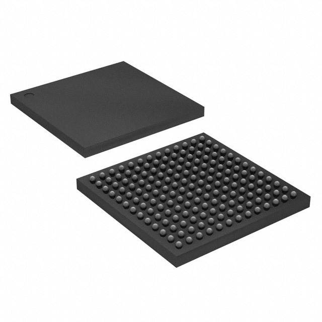
Figure 1 – 10M16SAU169C8G 169-ball UBGA package (source: SnapEDA).
Pin categories include dedicated JTAG pins (TCK, TDI, TDO, TMS), configuration pins (nCONFIG, nSTATUS, CONF_DONE), analog input pins (ADC_VINx), clock input pins, and general-purpose I/O arranged across I/O banks. Designers should consult the Intel MAX 10 Pin Connection Guidelines for proper power and ground connections during layout.
4. Block Diagram & Internal Architecture
The MAX 10 architecture centers around an array of Logic Array Blocks (LABs), each containing 16 logic elements with a 4-input LUT and programmable register. Surrounding the logic fabric are embedded M9K memory blocks (549 Kb total), 18 × 18 embedded multipliers for DSP operations, and a flexible clock network driven by 4 PLLs.
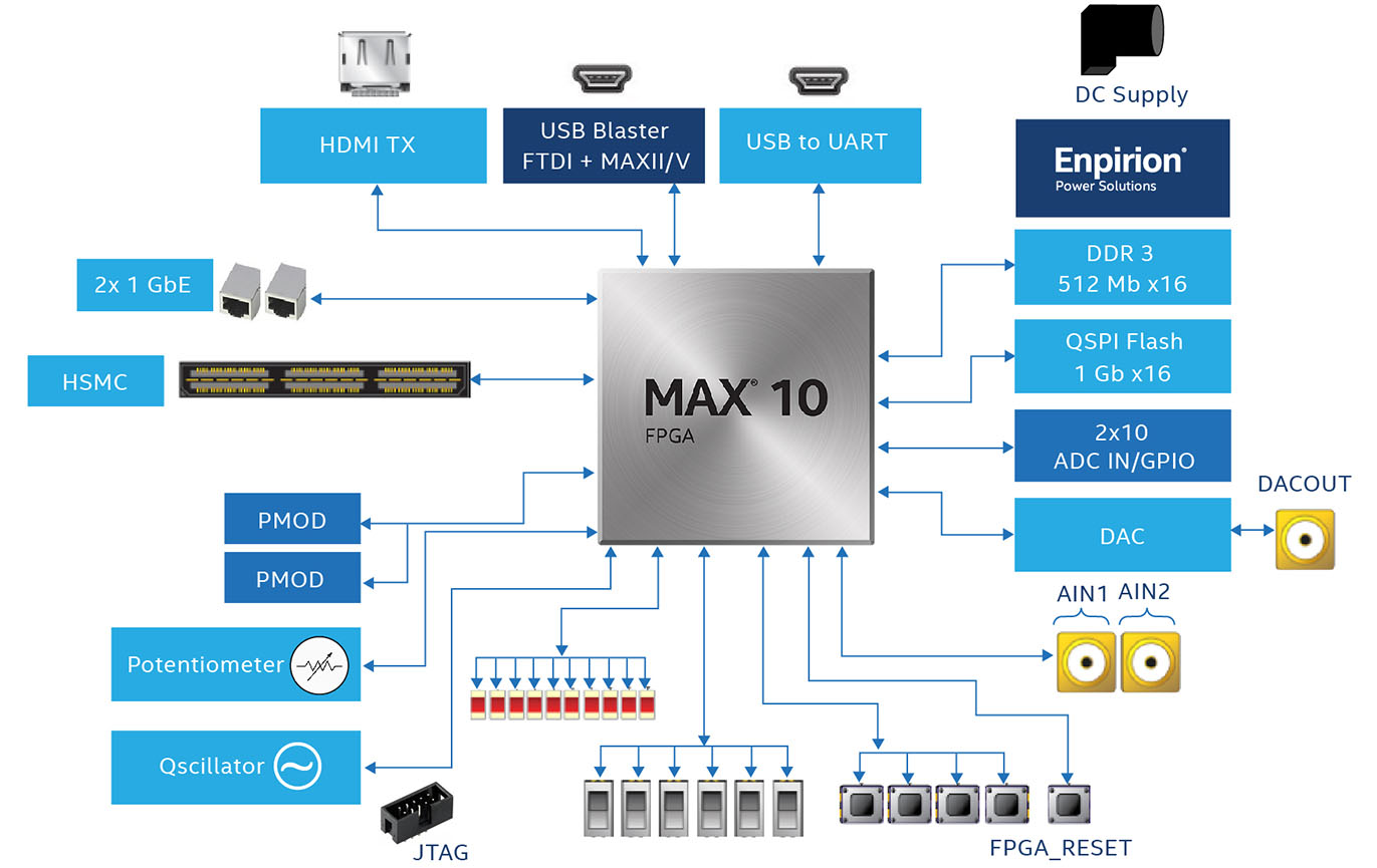
Figure 2 – MAX 10 FPGA architecture block diagram (source: Altera).
A distinguishing feature is the integrated 12-bit ADC block, which supports up to 18 single-ended analog input channels at up to 1 MSPS. The ADC interfaces directly with the FPGA fabric through a dedicated internal bus, enabling low-latency sensor data acquisition without external components. Dual configuration flash images allow safe remote firmware updates—if the new image fails, the device automatically reverts to the golden image.
5. Application Circuit & Design Guide
A minimal 10M16SAU169C8G design requires the following power supplies: 1.2 V (VCC core), 2.5 V (VCCA for PLLs), and bank-specific VCCIO rails (typically 3.3 V for LVTTL or 2.5 V for LVCMOS). Intel recommends 100 nF decoupling capacitors on each supply pin and a bulk 10 µF capacitor near each regulator output.
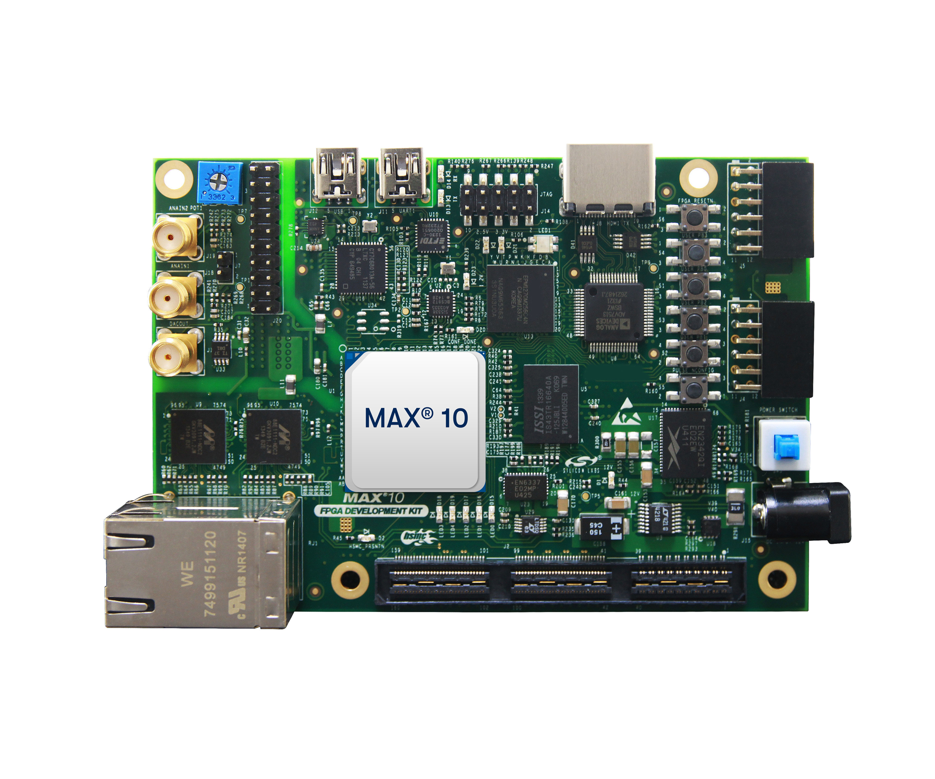
Figure 3 – MAX 10 FPGA Development Kit demonstrating a reference application circuit (source: Altera).
The JTAG header (TCK, TDI, TDO, TMS with 10 kΩ pull-ups) provides in-system programming via Intel Quartus Prime Programmer. For production, the internal flash can be programmed through JTAG or using the Parallel Flash Loader (PFL) IP core. Typical applications include:
- Industrial motor control – leveraging the ADC for current sensing and PWM generation through I/O
- IoT sensor hubs – using the ADC to digitize multiple sensor inputs, processing data in the FPGA fabric, and communicating via SPI/I²C/UART soft-core peripherals
- LED signage and display drivers – taking advantage of the high I/O count and instant-on capability
- Prototyping and education – supported by free Quartus Prime Lite Edition with full synthesis and simulation
For rapid prototyping, Intel offers the MAX 10 FPGA Evaluation Kit and third-party boards like the Alorium Snō module and Terasic maXimator.
Video Tutorial: Getting Started with MAX 10 FPGA
6. Frequently Asked Questions (FAQ)
Q1: What is the 10M16SAU169C8G?
The 10M16SAU169C8G is a non-volatile FPGA from Intel's MAX 10 family. It contains 16,000 logic elements, 549 Kb M9K embedded memory, 2,304 Kb user flash memory, and an integrated 12-bit ADC, all housed in a 169-ball UBGA package.
Q2: Does the 10M16SAU169C8G require external configuration memory?
No. The MAX 10 stores its configuration in internal flash memory, providing instant-on operation. No external EEPROM, SPI flash, or configuration PROM is needed, reducing BOM cost and board space.
Q3: What is the operating temperature range?
The C8G speed grade operates from 0 °C to +85 °C (commercial temperature range). For extended temperature (−40 °C to +100 °C), consider the "I" temperature grade variants such as the 10M16SAU169I7G.
Q4: How do I program the 10M16SAU169C8G?
Programming is performed through the JTAG interface using the Intel Quartus Prime Programmer (included in the free Lite Edition). The device supports in-system programming, and dual configuration images enable safe over-the-air updates with automatic fallback.
Q5: What development tools are available?
Intel Quartus Prime Lite Edition (free) provides full synthesis, place-and-route, timing analysis, and simulation for all MAX 10 devices. The Platform Designer (formerly Qsys) tool enables system-level integration of soft-core processors (Nios II), memory controllers, and communication peripherals.
Q6: Can the integrated ADC replace an external ADC chip?
In many applications, yes. The on-chip 12-bit ADC supports up to 18 analog input channels at 1 MSPS with a 0–3.3 V input range. For applications requiring higher resolution (14-bit+), higher sample rates, or differential inputs, an external ADC may still be necessary.


