
10M16SAU169I7G Datasheet, Specifications & Application Guide – Altera MAX 10 FPGA
The 10M16SAU169I7G is a non-volatile FPGA from the Altera (Intel) MAX 10 family, built on a 55 nm flash process. Featuring 16,000 logic elements, an integrated dual 12-bit ADC, and internal configuration flash, it delivers instant-on operation for industrial IoT, motor control, and mixed-signal embedded designs. This guide covers the full datasheet specifications, pinout, block diagram, application circuits, and design tips for the 10M16SAU169I7G.
1. 10M16SAU169I7G Overview & Part Number Decode
The 10M16SAU169I7G belongs to the MAX 10 FPGA family originally developed by Altera (now part of Intel, operating under the Altera brand). MAX 10 is the industry's first single-chip, non-volatile FPGA built on a 55 nm flash process node. The on-chip configuration flash eliminates external configuration devices and enables instant-on power-up in milliseconds.
Part number breakdown:
- 10M16 – MAX 10 family, 16,000 logic elements
- S – Single power-supply (integrated 1.2 V core regulator)
- A – Analog block enabled (dual 12-bit ADC)
- U169 – 169-ball UBGA package (11 × 11 mm)
- I – Industrial temperature range (−40 °C to +100 °C)
- 7 – Speed grade 7
- G – Lead-free (RoHS compliant)
The single-supply "S" variant simplifies board design—only a 3.3 V input is required. The internal voltage regulator generates the 1.2 V core supply, reducing BOM cost and PCB area. For related MAX 10 variants, see our guides on the 10M16SAU169C8G (commercial grade) and the 10M08SAE144C8G (8K LE, 144-EQFP variant).
2. Key Specifications & Electrical Parameters
| Parameter | Value |
|---|---|
| Part Number | 10M16SAU169I7G |
| Family | Altera (Intel) MAX 10 |
| Process Node | 55 nm Flash |
| Logic Elements (LEs) | 16,000 |
| Logic Array Blocks (LABs) | 1,000 |
| Embedded Memory (M9K RAM) | 549 Kb |
| User Flash Memory (UFM) | 2,304 Kb |
| 18 × 18 DSP Multipliers | 45 |
| PLLs | 4 |
| ADC | Dual 12-bit SAR, up to 1 MSPS |
| Max Analog Input Channels | 18 |
| Maximum User I/O | 130 |
| LVDS Pairs | Up to 22 |
| I/O Standards | 3.3 V / 2.5 V / 1.8 V / 1.5 V / 1.2 V LVCMOS, LVTTL, SSTL, HSTL, LVDS |
| Core Voltage | 1.2 V (internally regulated) |
| Supply Voltage | 3.0 V – 3.6 V single supply |
| Operating Temperature | −40 °C to +100 °C (Industrial) |
| Speed Grade | 7 (Slowest / Lowest Power) |
| Package | 169-ball UBGA (11 × 11 mm, 0.8 mm pitch) |
| Configuration | Internal flash, dual-image with remote update |
| Bitstream Security | AES-128 encryption |
| RoHS | Compliant (Lead-free) |
The speed grade 7 is the slowest (and lowest-power) option in the MAX 10 lineup. For timing-critical designs, consider speed grade 6 variants. All MAX 10 devices are supported by the free Quartus Prime Lite Edition.
3. Block Diagram & Internal Architecture
The MAX 10 architecture integrates programmable logic, embedded memory, DSP blocks, PLLs, a dual ADC, and user flash memory into a single monolithic die. The block diagram below illustrates the key functional blocks of the MAX 10 development platform:
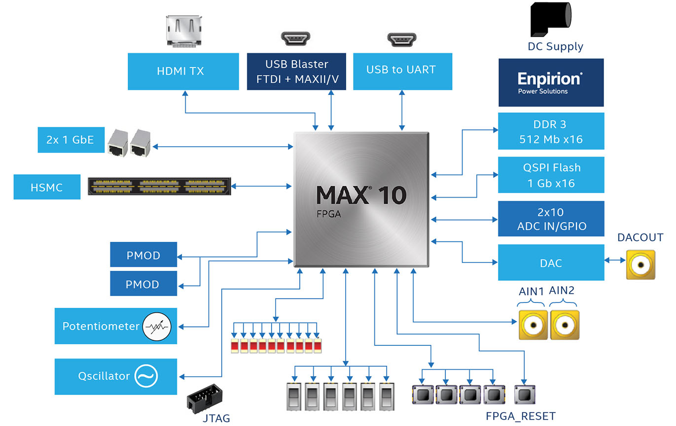
Architecture highlights:
- Logic Array Blocks (LABs): 1,000 LABs, each containing 16 Adaptive Logic Modules (ALMs) with look-up tables, registers, and carry chains.
- M9K Memory Blocks: 549 Kb of dual-port embedded SRAM configurable as ROM, single-port RAM, dual-port RAM, or FIFO.
- DSP Blocks: 45 embedded 18 × 18 multipliers supporting multiply-accumulate (MAC), FIR filters, and FFT operations.
- Dual ADC: Two independent 12-bit successive-approximation ADCs sharing up to 18 analog input channels, with internal temperature sensor and voltage monitoring.
- Configuration Flash: Dual-image support enables safe remote firmware updates with automatic fallback to a known-good image.
- PLLs: Four general-purpose PLLs supporting clock multiplication, division, and phase shifting up to 500 MHz.
4. Pinout, Package & Footprint
The 10M16SAU169I7G is housed in a 169-ball UBGA (Ultra-thin Ball Grid Array) package measuring 11 × 11 mm with a 0.8 mm ball pitch. The compact form factor makes it ideal for space-constrained designs in IoT and industrial applications.

Pin categories for the U169 package:
- User I/O: Up to 130 general-purpose I/O pins across 6 I/O banks
- Dedicated Clock Inputs: 4 dedicated clock input pins for low-jitter clocking
- JTAG: TDI, TDO, TMS, TCK for programming and boundary scan
- Configuration: nSTATUS, nCONFIG, CONF_DONE for configuration status
- Analog: Dedicated ADC input pins (shared with digital I/O)
- Power/Ground: Multiple VCC, VCCIO, and GND balls for clean power distribution
For complete pin assignment files in CSV/TXT format, visit the official Altera Pin-Out Files page. Explore more MAX 10 options on WWDParts FPGA Collections.
5. Application Circuits & Design Examples
The MAX 10 FPGA family targets a wide range of embedded applications. The integrated ADC, instant-on flash, and single-supply operation make the 10M16SAU169I7G especially suited for:
- Industrial control & motor drives – PWM generation, encoder interfaces, real-time sensor fusion
- IoT edge gateways – Protocol bridging (SPI/I2C/UART to Ethernet), sensor aggregation
- Video surveillance preprocessing – MIPI CSI-2 interface, image scaling, overlay generation
- Medical instrumentation – Multi-channel ADC data acquisition, digital filtering
- Test & measurement – Custom logic analyzers, waveform generators
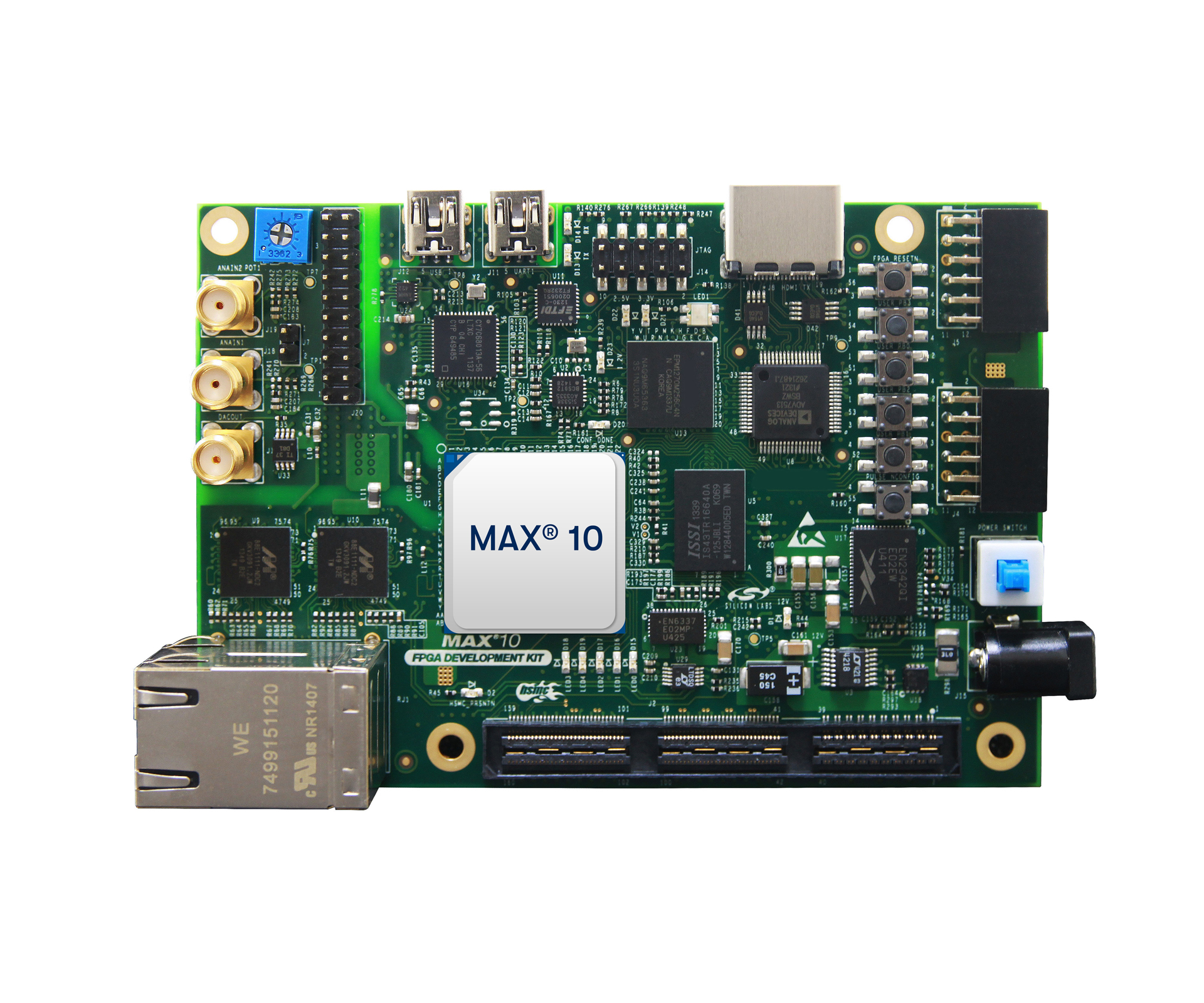
The MAX 10 FPGA Development Kit shown above provides a complete reference design including USB-Blaster II programming, DDR3 memory, Ethernet, and Arduino/PMOD expansion headers. It serves as an excellent starting point for prototyping 10M16SAU169I7G-based designs.
Typical Application Circuit Considerations
- Power supply: A single 3.3 V rail feeds VCC and all VCCIO banks. Add 100 nF decoupling capacitors on every power ball and 10 µF bulk capacitors near the device.
- Configuration: Internal flash provides instant-on. For JTAG programming, connect TDI, TDO, TMS, TCK to the USB-Blaster header.
- ADC inputs: Use 100 Ω series resistors and 100 nF filter capacitors on analog input channels. Route analog traces away from high-speed digital signals.
- Clock: A 50 MHz oscillator feeding a dedicated clock input, multiplied internally by PLL to the desired system frequency.
Video Tutorial: Getting Started with MAX 10 FPGA
6. FAQ – Frequently Asked Questions
What is the 10M16SAU169I7G?
The 10M16SAU169I7G is a non-volatile FPGA from the Altera MAX 10 family with 16,000 logic elements, a dual 12-bit ADC, 549 Kb embedded RAM, 2,304 Kb user flash memory, and 45 DSP multipliers in a 169-ball UBGA package. It operates across the industrial temperature range of −40 °C to +100 °C.
Does the 10M16SAU169I7G require an external configuration device?
No. The MAX 10 family stores configuration data in on-chip flash memory, eliminating the need for an external EEPROM or flash chip. The device supports dual configuration images for safe remote updates with automatic fallback.
What supply voltage does the 10M16SAU169I7G need?
The "S" (single-supply) variant requires only a 3.0 V to 3.6 V input. An integrated voltage regulator generates the 1.2 V core supply internally, simplifying power design and reducing BOM cost.
What is the difference between the I7G and C8G variants?
The "I7G" suffix denotes industrial temperature (−40 °C to +100 °C) at speed grade 7. The "C8G" variant operates in the commercial temperature range (0 °C to +85 °C) at speed grade 8. The I7 variant offers wider temperature tolerance while the C8 provides faster timing.
What software tools support the 10M16SAU169I7G?
All MAX 10 devices are fully supported by the free Quartus Prime Lite Edition, which provides synthesis, place-and-route, timing analysis, and JTAG programming. No paid license is required for MAX 10 development.
How many ADC channels does the 10M16SAU169I7G have?
The device integrates two independent 12-bit successive-approximation ADCs that share up to 18 analog input channels. Each ADC supports up to 1 MSPS sampling rate with an internal temperature sensor and voltage monitoring capability.


