
10M04SCE144C8G Datasheet, Pinout, Specifications & Application Guide | Intel MAX 10 FPGA
The 10M04SCE144C8G is a non-volatile, single-chip FPGA from Intel's (formerly Altera) MAX 10 family, built on 55 nm flash process technology. With 4,000 logic elements, 189 Kb of embedded SRAM, an integrated 12-bit ADC, and internal dual-image configuration flash, it delivers instant-on capability in a compact 144-pin EQFP package. Designed for cost-sensitive industrial, IoT, and consumer applications, the 10M04SCE144C8G eliminates the need for external configuration memory, reducing both board area and BOM cost.
Key Specifications & Parameters
The table below summarizes the core electrical, physical, and functional parameters of the 10M04SCE144C8G. All values are taken from the official Intel MAX 10 device handbook and distributor datasheets.
| Parameter | Value |
|---|---|
| Manufacturer | Intel (Altera) |
| Family | MAX 10 (10M04) |
| Process Technology | 55 nm Flash |
| Logic Elements (LEs) | 4,000 |
| Embedded SRAM | 189 Kb (M9K blocks) |
| User Flash Memory (UFM) | Up to 256 Kb |
| PLLs | 2 |
| 18 × 18 Embedded Multipliers | 16 |
| Analog-to-Digital Converter | 1× 12-bit ADC (up to 1 MSPS) |
| Maximum User I/O (E144 package) | 101 |
| Maximum LVDS Pairs | 15 |
| Package | 144-EQFP (Exposed Pad), 20 × 20 mm |
| Core Supply Voltage | 1.2 V (1.15 V – 1.25 V) |
| I/O Voltage | 3.3 V / 2.5 V / 1.8 V / 1.5 V / 1.2 V |
| Speed Grade | 8 (commercial) |
| Operating Temperature | 0 °C to +85 °C (commercial) |
| Configuration | Internal dual-image flash (instant-on) |
| Supported I/O Standards | LVTTL, LVCMOS, SSTL, HSTL, LVDS, RSDS, Mini-LVDS |
| RoHS Compliance | Yes (EU 2011/65/EU) |
The single-supply variant (indicated by the "S" in the part number) simplifies power design by requiring only a 3.3 V external supply; the on-chip voltage regulator generates the 1.2 V core rail internally.
Block Diagram & Architecture
The MAX 10 architecture integrates programmable logic, embedded memory, DSP blocks, a configurable ADC, and dual configuration-flash memory into a single monolithic die. The diagram below illustrates the high-level functional blocks inside the 10M04SCE144C8G.
Key architectural highlights include:
- Logic Array Blocks (LABs): Each LAB contains 10 adaptive logic modules (ALMs) with look-up tables, registers, and carry chains.
- M9K Memory Blocks: 9-Kb SRAM blocks configurable as single- or dual-port RAM, ROM, or FIFO.
- DSP Blocks: Hardened 18×18 multipliers supporting multiply-accumulate for signal-processing pipelines.
- Analog-to-Digital Converter: Integrated 12-bit SAR ADC with up to 18 analog input channels and a dedicated temperature-sensing diode.
- Configuration Flash Memory (CFM): Stores two configuration images, enabling remote field updates with a known-good fallback image.
Pinout & Package Information
The 10M04SCE144C8G uses a 144-pin EQFP package with an exposed thermal pad on the underside. The package measures 20 × 20 mm with a 0.5 mm lead pitch, making it compatible with standard SMT assembly processes.
Pin categories include:
- User I/O Pins: Up to 101 general-purpose I/O pins across 4 I/O banks, each independently configurable for voltage level and I/O standard.
- JTAG Pins: TCK, TMS, TDI, TDO for boundary-scan testing and in-system programming.
- Configuration Pins: DCLK, DATA0, nCONFIG, nSTATUS, CONF_DONE for device configuration.
- Power Pins: VCC (1.2 V core), VCCIO (per-bank I/O supply), VCCA (PLL analog supply).
- Analog Inputs: Dedicated ADC input pins shared with certain I/O pins.
For the complete pin-to-signal mapping, refer to the Intel MAX 10 Device Handbook.
Typical Applications & Circuit Design
The 10M04SCE144C8G is well suited for a range of embedded applications where instant-on behavior, integrated analog, and low power consumption are critical.

Common application areas include:
- Industrial Automation: Motor-control interfaces, sensor hubs, and programmable logic controllers using the onboard ADC for analog sensor acquisition.
- IoT Edge Devices: Protocol bridging (SPI/I²C/UART), local data pre-processing, and low-latency decision-making at the network edge.
- Board Management Controllers: Power sequencing, voltage/current monitoring via the ADC, and system health reporting.
- Video & Display: LVDS serializer/deserializer for flat-panel displays, image overlay, and format conversion.
- Communications: Custom serial transceivers, CRC/ECC engines, and packet-processing accelerators.
A minimal design requires only a 3.3 V supply, decoupling capacitors, and a JTAG header for programming. The on-chip configuration flash eliminates the BOM line item for external serial NOR flash.
Design Resources & Development Tools
Intel provides comprehensive free tooling for the MAX 10 family:
- Quartus Prime Lite Edition: Full synthesis, place-and-route, timing analysis, and the Platform Designer (formerly Qsys) system integration tool — completely free with no license file required.
- ModelSim Intel FPGA Starter Edition: RTL and gate-level simulation bundled with Quartus Prime Lite.
- Nios II Soft Processor: 32-bit embedded processor IP that runs inside the FPGA fabric, with a full software IDE and HAL library.
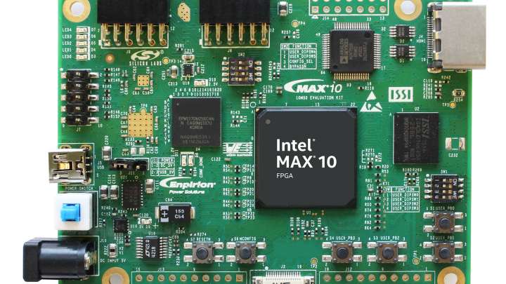
- MAX 10 Development Kit: Reference board with the 10M50 device, Arduino-compatible headers, and onboard USB-Blaster — ideal for prototyping designs portable to the 10M04.
The following video provides a practical walkthrough for getting started with Intel MAX 10 FPGA development:
For schematic symbols and PCB footprints, visit SnapEDA to download ready-to-use library files for Altium Designer, KiCad, Eagle, and OrCAD.
Related Intel MAX 10 FPGA Articles on WWDParts
- 10M08SAE144C8G Datasheet, Pinout & Specifications — Intel MAX 10 FPGA
- 10M16SAU169C8G Datasheet, Specs & Pinout — Intel MAX 10 FPGA
- 10M16SAU169I7G Datasheet & Application Guide — Altera MAX 10 FPGA
Frequently Asked Questions (FAQ)
1. What is the difference between 10M04SCE144C8G and 10M04DCE144C8G?
The "S" in 10M04SCE144C8G denotes the single-supply variant, which includes an on-chip voltage regulator to generate the 1.2 V core supply from a single 3.3 V rail. The "D" variant (dual-supply) requires an external 1.2 V supply in addition to 3.3 V, but offers lower static power consumption and is preferred for battery-powered designs.
2. Does the 10M04SCE144C8G include an analog-to-digital converter?
Yes. It integrates one 12-bit SAR ADC capable of up to 1 MSPS with up to 18 analog input channels. The ADC is controlled through a dedicated hard IP block and can be used alongside the FPGA logic for mixed-signal designs.
3. How many configuration images can the 10M04SCE144C8G store internally?
The device supports dual configuration images stored in its internal configuration flash memory (CFM). This enables remote field updates with automatic fallback to the factory image if the new image fails to load, improving system reliability.
4. What software do I need to program the 10M04SCE144C8G?
Use Intel Quartus Prime Lite Edition, which is free and supports all MAX 10 devices without a license file. Programming is done via JTAG using an Intel USB-Blaster or compatible programmer. The Quartus Programmer utility generates and downloads .pof files directly to the on-chip flash.
5. Can I run an embedded processor inside the 10M04SCE144C8G?
Yes. The Nios II/e (economy) soft processor fits comfortably within 4,000 LEs and uses the on-chip M9K blocks as instruction/data memory. While the 10M04 is too small for the full-featured Nios II/f, the economy variant provides a 32-bit CPU suitable for simple control tasks and state machines.
6. What is the maximum operating frequency of the 10M04SCE144C8G?
The speed grade 8 device supports fabric clock frequencies up to approximately 300 MHz for register-to-register paths, depending on design complexity and routing. The two on-chip PLLs can generate output clocks from 16 MHz to 500 MHz from a wide input reference range.


