
10M16SAU169C8G Datasheet, Pinout, Specifications & Application Guide | Intel MAX 10 FPGA
The 10M16SAU169C8G is an Intel (Altera) MAX 10 FPGA featuring 16,000 logic elements, an integrated 12-bit ADC with up to 18 analog input channels, and dual configuration flash memory in a compact 169-ball UBGA package. Built on 55nm flash-based process technology, the "SA" variant operates from a single 3.3V power supply with internal voltage regulators, delivering instant-on non-volatile operation ideal for industrial automation, sensor fusion, and IoT edge computing. This comprehensive guide covers its pinout, key specifications, block diagram, and real-world application circuits to help engineers evaluate and integrate the 10M16SAU169C8G into their next design.
Overview & Key Features
The 10M16SAU169C8G belongs to the Intel MAX 10 FPGA family, the industry's first single-chip programmable logic device to integrate flash memory, analog-to-digital conversion, and configurable I/O in a non-volatile FPGA architecture. Unlike SRAM-based FPGAs, the MAX 10 retains its configuration in on-chip flash, enabling instant-on operation without an external configuration device.
Key features of the 10M16SAU169C8G include:
- 16,000 Logic Elements (LEs) — sufficient for complex digital designs including Nios II soft processors, protocol bridges, and multi-channel sensor interfaces
- Integrated 12-bit ADC — 1 MSPS sampling rate with up to 18 analog input channels, eliminating the need for an external ADC IC
- 549 Kb Embedded SRAM — M9K memory blocks configurable as RAM, ROM, or FIFO for high-bandwidth data buffering
- 2,304 Kb User Flash Memory (UFM) — on-chip non-volatile storage for calibration data, firmware, or configuration parameters
- Dual Configuration Flash — supports dual-image boot for remote update and fail-safe fallback operation
- Single 3.3V Supply — internal voltage regulators generate the 1.2V core supply, simplifying power design
- Instant-On Operation — non-volatile configuration flash allows the FPGA to be operational within milliseconds of power-up
The MAX 10 family is supported by Intel Quartus Prime Lite Edition, a free development environment that includes synthesis, place-and-route, simulation, and programming tools. For related Intel FPGA devices, see our guides on the 10M08SAE144C8G and 10M04SCE144C8G.
Technical Specifications
| Parameter | Value |
|---|---|
| Manufacturer | Intel (Altera) |
| Family | MAX 10 FPGA |
| Part Number | 10M16SAU169C8G |
| Logic Elements (LEs) | 16,000 |
| Embedded Memory (M9K) | 549 Kb |
| User Flash Memory (UFM) | 2,304 Kb |
| 18×18 Multipliers | 45 |
| PLLs | 4 |
| ADC Blocks | 1 (12-bit SAR, 1 MSPS) |
| Analog Input Channels | Up to 18 |
| Maximum User I/O Pins | 130 |
| Maximum LVDS Pairs | 22 |
| I/O Standards | 3.3V LVTTL, 1.0–3.3V LVCMOS, SSTL, HSTL, HSUL, LVDS |
| External Memory Interface | DDR2, DDR3, LPDDR2, SRAM |
| Package | 169-ball UBGA (Ultra-thin Ball Grid Array) |
| Package Dimensions | 11 mm × 11 mm |
| Core Voltage (VCC) | 1.2V (internally regulated) |
| PLL Supply (VCCA) | 2.5V |
| I/O Voltage (VCCIO) | 1.2V / 1.5V / 1.8V / 2.5V / 3.3V (bank-selectable) |
| Process Technology | 55 nm Flash |
| Speed Grade | C8 (commercial, standard speed) |
| Temperature Range | 0°C to 85°C (commercial) |
| Configuration | Dual-image internal flash, JTAG |
| RoHS Compliant | Yes (Pb-free, “G” suffix) |
Pinout & Package Information
The 10M16SAU169C8G is housed in a 169-ball Ultra-thin Ball Grid Array (UBGA) measuring 11 mm × 11 mm. The compact BGA footprint makes it suitable for space-constrained designs such as wearables, IoT modules, and small-form-factor industrial controllers. The 130 user I/O pins are organized across multiple I/O banks, each independently configurable for different voltage standards.

Pin Categories:
- VCC — 1.2V core supply (internally regulated in SA variant from 3.3V input)
- VCCIO — I/O bank supply voltage (3.3V typical, bank-selectable from 1.2V to 3.3V)
- VCCA / VCCD_PLL — 2.5V PLL analog and digital supply pins
- ANAIN1–ANAIN8 — dedicated analog input pins for the integrated 12-bit ADC
- CLK[0..3] — dedicated clock input pins routed to global clock networks
- JTAG (TCK, TMS, TDI, TDO) — programming and debug interface
- nSTATUS, nCONFIG, CONF_DONE — configuration status and control pins
- GND — ground pins distributed throughout the BGA for signal integrity
For the complete pin assignment table, use the Intel Quartus Prime Pin Planner tool or download the official MAX 10 FPGA pin-out files.
Block Diagram & Architecture
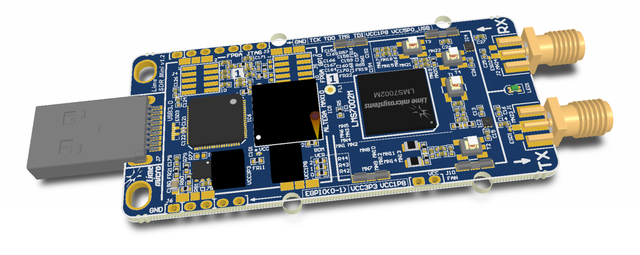
The MAX 10 FPGA architecture integrates programmable logic, embedded memory, clock management, analog-to-digital conversion, and configuration flash into a single monolithic die. The block diagram below illustrates the architecture of the LimeSDR-Mini, a popular software-defined radio board that uses the 10M16SAU169C8G as its primary FPGA:
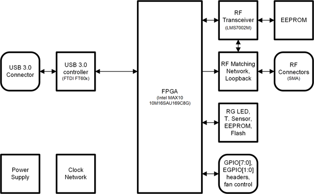
Architecture Highlights:
- Logic Array Blocks (LABs) — each LAB contains 16 Adaptive Logic Modules (ALMs) implementing combinational and sequential logic
- M9K Memory Blocks — configurable as single-port RAM, dual-port RAM, ROM, or FIFO for high-speed data buffering
- 18×18 Multiplier Blocks — 45 hardware multipliers for DSP applications including FIR filters and FFT computations
- 4 PLLs — general-purpose phase-locked loops for clock synthesis, multiplication, division, and phase shifting
- ADC Block — single 12-bit SAR ADC with multiplexed analog inputs and internal temperature sensor
- Configuration Flash Memory (CFM) — stores up to two FPGA configuration images for instant-on and remote update
- User Flash Memory (UFM) — 2,304 Kb of general-purpose non-volatile storage accessible from the FPGA fabric
Application Circuit & Design Guide
The 10M16SAU169C8G is used in a wide range of applications including software-defined radio, industrial control, motor drives, sensor hubs, and IoT edge devices. The LimeSDR-Mini development board shown below is a notable application of this FPGA, providing a complete SDR platform:
Typical Application Areas:
- Software-Defined Radio (SDR) — the LimeSDR-Mini pairs the 10M16SAU169C8G with a LMS7002M RF transceiver for full-duplex 10 MHz–3.5 GHz operation
- Sensor Fusion & Data Acquisition — the integrated ADC enables direct connection of analog sensors without external ADC ICs, reducing BOM cost
- Motor Control — hardware PWM generation combined with ADC feedback creates a compact single-chip motor controller
- Protocol Bridge / Interface Conversion — implement SPI-to-I2C, UART-to-Ethernet, or custom serial protocol converters
- IoT Edge Processing — Nios II soft processor combined with the ADC enables edge analytics and local decision-making
Power Supply Design Tips:
- Use the single 3.3V supply configuration (SA variant) to minimize power rails and simplify PCB routing
- Place 100 nF decoupling capacitors on each VCC and VCCIO pin, with a bulk 10 µF capacitor near each voltage regulator
- Enable the internal oscillator for applications that do not require high clock accuracy, eliminating an external crystal
- Leverage dual-image configuration flash for over-the-air firmware updates with automatic fallback to a known-good image
Video Tutorial: Getting Started with Intel MAX 10 FPGA
For more FPGA development resources, explore our guides on Xilinx Artix-7 XC7A35T-1CPG236C and other popular FPGA devices.
Frequently Asked Questions
What is the difference between 10M16SAU169C8G and 10M16SCU169C8G?
The “SA” in 10M16SAU169C8G indicates a single-supply analog variant with an integrated 12-bit ADC and internal voltage regulators, requiring only a single 3.3V supply. The “SC” variant (10M16SCU169C8G) is a single-supply core-only version without the ADC block. Choose the SA variant when your design requires analog-to-digital conversion; choose SC for digital-only designs at a lower cost.
What development tools are needed to program the 10M16SAU169C8G?
You need Intel Quartus Prime Lite Edition (free download) for design entry, synthesis, and programming. A USB Blaster or USB Blaster II programmer is required for JTAG-based configuration. The Quartus Prime software includes the Nios II Embedded Design Suite for soft processor development and ModelSim-Intel FPGA Starter Edition for simulation.
How does the 10M16SAU169C8G compare to the 10M08SAE144C8G?
The 10M16SAU169C8G offers twice the logic capacity (16,000 vs 8,000 LEs), more embedded memory (549 Kb vs 378 Kb), more user flash (2,304 Kb vs 256 Kb), 4 PLLs vs 2, and 130 I/O pins vs 101. It uses a 169-ball UBGA package instead of 144-pin EQFP, which is more compact but requires BGA-capable PCB manufacturing. Both share the same 12-bit ADC, 55nm process, and C8 speed grade.
Can the 10M16SAU169C8G be used without an external configuration memory?
Yes. The MAX 10 FPGA has on-chip configuration flash memory that stores up to two configuration images. This eliminates the need for external configuration PROMs or SPI flash devices. The device supports instant-on operation, booting from internal flash within milliseconds of power-up, and dual-image boot enables safe remote firmware updates with automatic fallback.
What is the LimeSDR-Mini and how does it use the 10M16SAU169C8G?
The LimeSDR-Mini is an open-source software-defined radio (SDR) board that uses the 10M16SAU169C8G as its FPGA for digital signal processing. It pairs the FPGA with a Lime Microsystems LMS7002M RF transceiver, providing full-duplex operation from 10 MHz to 3.5 GHz with USB 3.0 connectivity. The FPGA handles baseband processing, data streaming, and control logic, demonstrating the 10M16SAU169C8G's capability in demanding RF applications.
What is the maximum operating frequency and power consumption of the 10M16SAU169C8G?
The 10M16SAU169C8G (C8 speed grade) supports maximum internal clock frequencies up to 300 MHz for simple register-to-register paths, with 4 on-chip PLLs generating clock frequencies from approximately 5 MHz to 472.5 MHz. Typical static power consumption is around 45–60 mW, with dynamic power depending on clock frequency, toggle rate, and resource utilization. Use the Intel PowerPlay Early Power Estimator tool for accurate power estimates.


