
10M16SAU169I7G Datasheet, Specifications & Application Guide – Altera MAX 10 FPGA
The 10M16SAU169I7G is a non-volatile FPGA from the Altera (Intel) MAX 10 family, fabricated on a 55 nm flash process. It integrates 16,000 logic elements, a dual 12-bit analog-to-digital converter (ADC), 2,304 Kb of user flash memory, and internal configuration storage — enabling true instant-on operation without an external configuration device. Housed in a compact 169-ball UBGA package with an industrial temperature rating of −40 °C to +100 °C, the 10M16SAU169I7G targets cost-sensitive, mixed-signal embedded applications in industrial automation, IoT edge nodes, motor control, and sensor fusion.
1. Device Overview & Part Number Decode
The MAX 10 family is Altera's (now Intel's) single-chip, non-volatile FPGA platform. Unlike SRAM-based FPGAs that require external flash or PROM for configuration, MAX 10 devices store their bitstream in on-die flash, delivering power-on in milliseconds. The 10M16SAU169I7G sits in the mid-range of the family, balancing logic density and I/O count with a small footprint suitable for board-constrained designs.
Part number breakdown:
- 10M16 – MAX 10 family, 16,000 logic elements
- S – Single power-supply operation (no separate VCCIO rail needed for most banks)
- A – Analog block enabled (dual 12-bit ADC)
- U169 – 169-ball Ultra Fine-Line BGA (UBGA) package, 11 × 11 mm
- I – Industrial temperature grade (−40 °C to +100 °C)
- 7 – Speed grade 7 (lowest power variant in the MAX 10 line-up)
The single-supply and integrated ADC features make this device especially compelling for sensor-rich embedded systems where board space and BOM cost are critical. For related MAX 10 variants, see our guides on the 10M25SAE144C8G (144-EQFP) and 10M08SAE144C8G.
2. Key Specifications & Electrical Parameters
| Parameter | Value |
|---|---|
| Part Number | 10M16SAU169I7G |
| Family | Altera (Intel) MAX 10 |
| Process Node | 55 nm Flash |
| Logic Elements (LEs) | 16,000 |
| Logic Array Blocks (LABs) | 1,000 |
| Embedded Memory (M9K) | 549 Kb (61 blocks × 9 Kb) |
| User Flash Memory (UFM) | 2,304 Kb |
| 18 × 18 DSP Multipliers | 45 |
| PLLs | 4 |
| ADC | Dual 12-bit, up to 1 MSPS each |
| Maximum User I/O Pins | 130 |
| LVDS Pairs | Up to 26 (package-dependent) |
| Package | 169-UBGA (11 × 11 × 1.0 mm, 0.8 mm pitch) |
| Core Supply Voltage (VCC) | 1.2 V (internal core) |
| I/O Supply Voltage (VCCIO) | 3.0 V / 3.3 V (bank-dependent) |
| Operating Temperature | −40 °C to +100 °C (Industrial) |
| Speed Grade | 7 (low-power) |
| Configuration | Internal flash (instant-on), JTAG, dual-image boot |
| I/O Standards Supported | LVCMOS, LVTTL, SSTL, HSTL, LVDS, differential SSTL |
| RoHS Compliant | Yes |
3. Block Diagram & Architecture
The MAX 10 architecture follows a column-based fabric layout. Logic Array Blocks (LABs), each containing 16 logic elements, are interleaved with columns of M9K embedded memory and 18 × 18 DSP multiplier blocks. Four PLLs sit at the device periphery to manage clock distribution, supporting frequencies up to 500 MHz. The integrated dual 12-bit ADC connects directly to dedicated analog input pins, enabling mixed-signal designs without external ADC ICs.
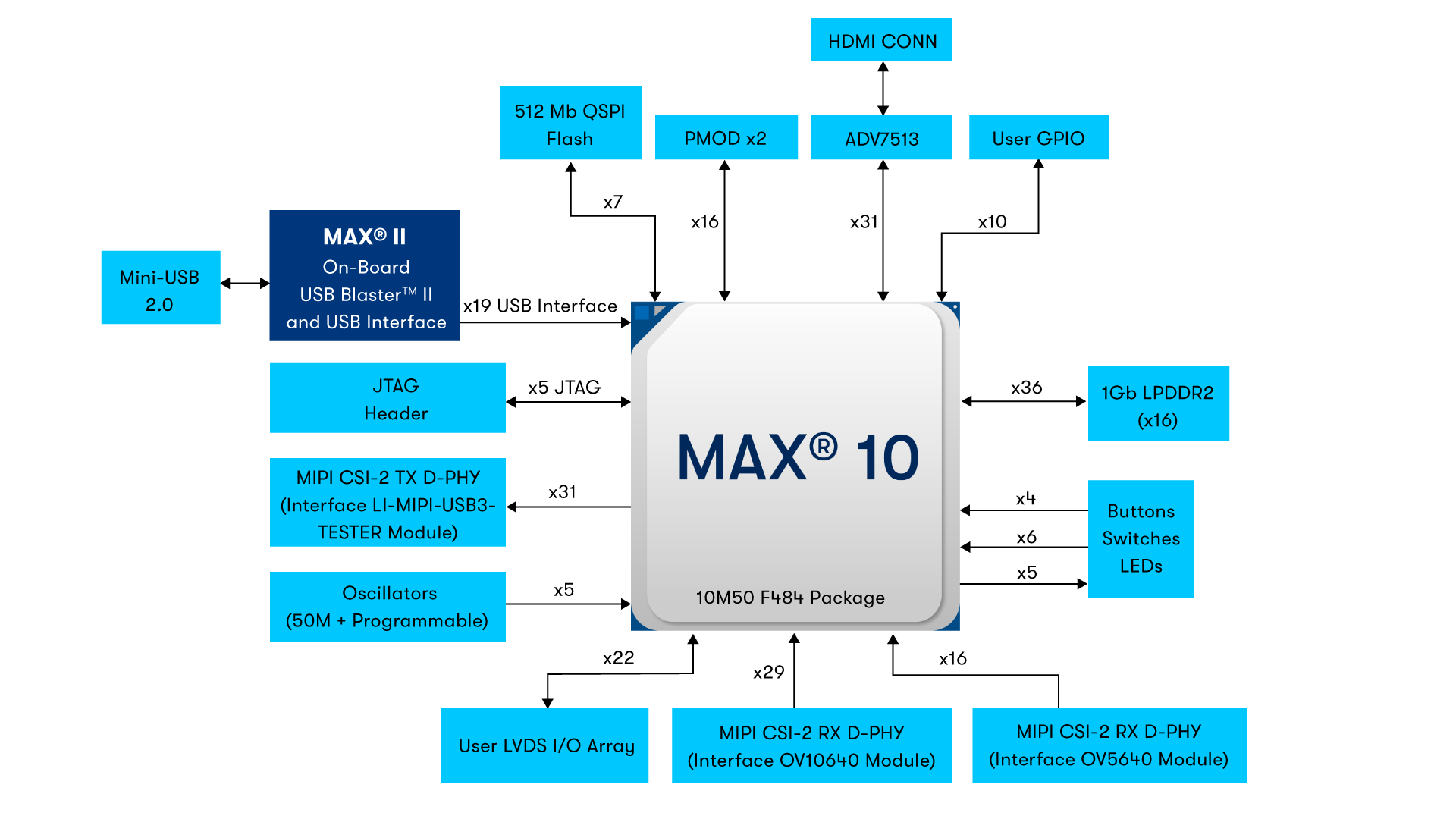
Figure 1: MAX 10 FPGA system block diagram illustrating the key functional blocks and interconnects.
Key architectural highlights include:
- Instant-on configuration – Bitstream stored in on-die flash; device is functional within milliseconds of power-up.
- Dual-image boot – Two configuration images can reside in flash for fail-safe remote updates.
- User Flash Memory (UFM) – 2,304 Kb available for storing calibration data, encryption keys, or boot parameters without external EEPROM.
- Integrated ADC – Two independent 12-bit ADC cores with up to 18 analog inputs, supporting 1 MSPS conversion for temperature sensing, voltage monitoring, or low-bandwidth signal acquisition.
4. Pinout & Package Information
The 10M16SAU169I7G uses a 169-ball UBGA package with a 0.8 mm ball pitch in an 11 × 11 mm body. This compact footprint makes it ideal for space-constrained PCB layouts. The 130 available user I/O pins are organized across multiple I/O banks, each independently configurable for voltage levels from 1.2 V to 3.3 V.

Figure 2: Altera MAX 10 FPGA in 169-UBGA package (representative U169 package photo).
Pin categories in the U169 package:
- User I/O – 130 general-purpose pins supporting LVCMOS, LVTTL, SSTL, HSTL, and LVDS standards
- Power (VCC / VCCIO / GND) – Dedicated core, I/O bank, and analog supply/ground pins
- Configuration (JTAG) – TDI, TDO, TMS, TCK for programming and boundary-scan testing
- Analog inputs – Dedicated pins routed to the internal dual 12-bit ADC block
- Clock inputs – Global and regional clock-capable pins feeding the four on-chip PLLs
For a complete ball map and recommended PCB land pattern, consult the Intel MAX 10 FPGA Device Architecture handbook. Also check our 10M16SAU169C8G guide for a comparison of the commercial-grade variant in the same package.
5. Application Circuits & Design Tips
The 10M16SAU169I7G is widely deployed in industrial automation, motor drives, sensor hubs, IoT gateways, video pre-processing pipelines, and medical instrumentation. Its integrated ADC eliminates external analog front-end components, while the single-supply architecture simplifies power rail design.
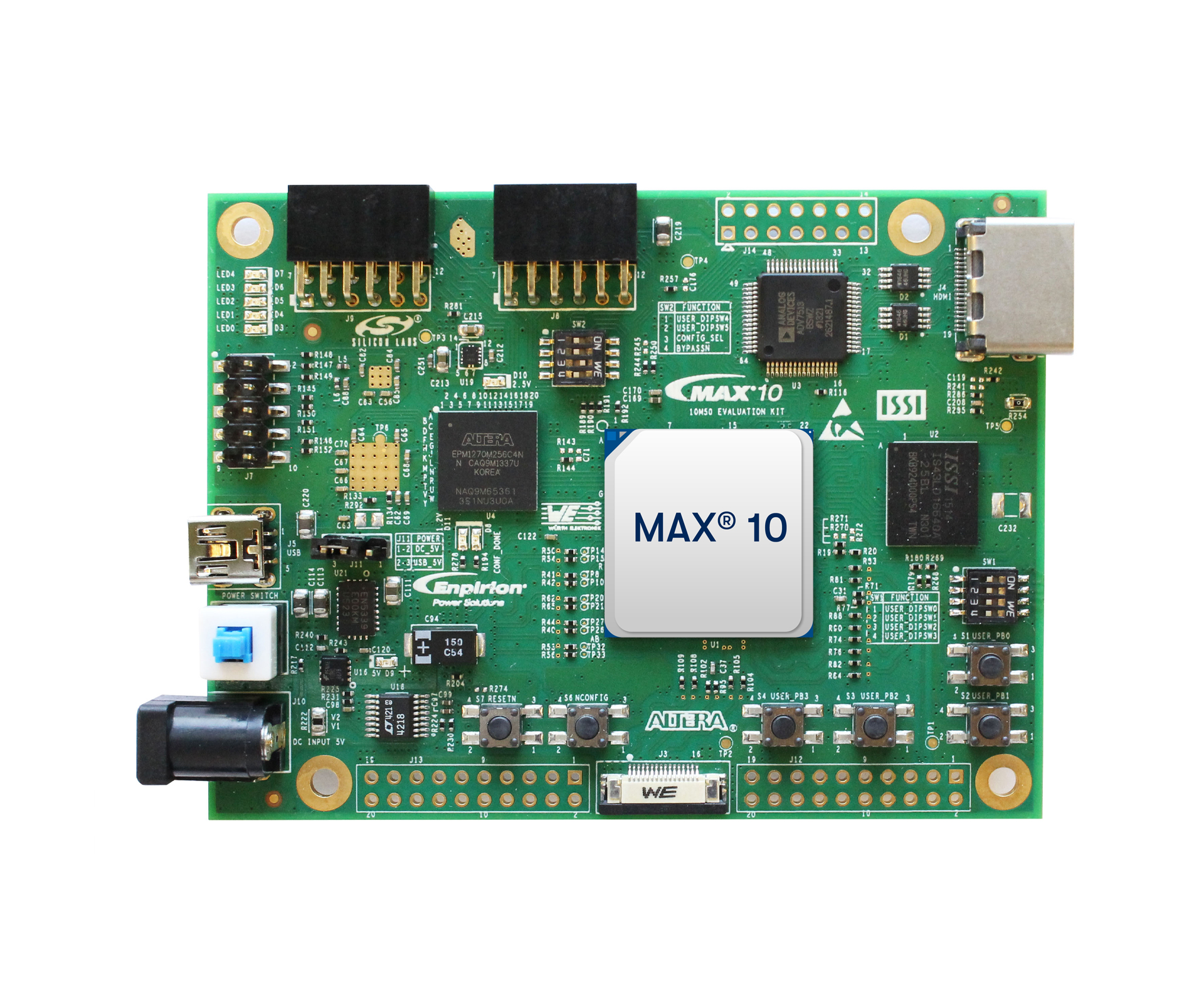
Figure 3: MAX 10 FPGA evaluation kit — a reference design platform demonstrating typical application circuitry.
Design recommendations:
- Power supply – Use a single 3.3 V rail with an integrated LDO or DC-DC converter to generate the 1.2 V core supply. Decouple each VCC and VCCIO pin with 100 nF MLCC capacitors placed as close to the BGA pads as possible.
- Configuration – For production, use internal flash configuration (no external PROM required). For development, JTAG via USB-Blaster provides rapid iteration. Enable dual-image boot for field-upgradable firmware with rollback protection.
- ADC integration – Route analog input traces away from digital switching noise. Use a dedicated analog ground plane partition under the ADC input pins. Apply anti-aliasing RC filters (e.g., 100 Ω + 100 pF) at each analog input.
- Thermal management – At industrial temperature limits, ensure adequate airflow or use thermal vias under the exposed pad to a ground plane for heat dissipation.
- ESD protection – All I/O pins have built-in ESD protection, but add TVS diodes on externally accessible connectors for IEC 61000-4-2 compliance.
Video Tutorial: Getting Started with Intel MAX 10 FPGA
6. Frequently Asked Questions (FAQ)
What is the 10M16SAU169I7G and what family does it belong to?
The 10M16SAU169I7G is a non-volatile FPGA from the Altera (Intel) MAX 10 family. Built on a 55 nm flash process, it integrates 16,000 logic elements, a dual 12-bit ADC, 2,304 Kb of user flash memory, and 549 Kb of embedded SRAM in a 169-ball UBGA package. Its on-chip configuration flash enables instant-on power-up without external memory devices.
What is the operating temperature range of the 10M16SAU169I7G?
The 10M16SAU169I7G is rated for the industrial temperature range of −40 °C to +100 °C, as indicated by the "I" suffix in its part number. This makes it suitable for harsh-environment applications including factory automation, outdoor IoT nodes, and automotive-adjacent systems.
Does the 10M16SAU169I7G include an analog-to-digital converter (ADC)?
Yes. The "A" in the part number denotes an enabled analog block. The device contains two independent 12-bit ADC cores, each capable of up to 1 MSPS, with up to 18 analog input channels available depending on pin configuration. This integrated ADC eliminates the need for external ADC chips in many mixed-signal designs.
What software tools are needed to program the 10M16SAU169I7G?
You can develop for the 10M16SAU169I7G using Intel Quartus Prime Lite Edition, which is available as a free download. Quartus Prime supports Verilog, VHDL, and schematic entry. Programming is done via JTAG using a USB-Blaster or compatible download cable. The Quartus Prime tool also includes the Platform Designer (formerly Qsys) system integration tool for building Nios II soft-processor and peripheral subsystems.
Can the 10M16SAU169I7G be used for dual-image boot and remote firmware updates?
Yes. The MAX 10 internal flash supports storing two configuration images, enabling a factory-safe image alongside an application image. If a remote update corrupts the application image, the device can automatically fall back to the factory image on the next power cycle. This dual-boot capability is essential for field-deployed systems requiring over-the-air (OTA) firmware updates with rollback protection.
What are the main differences between the 10M16SAU169I7G and the 10M16SAU169C8G?
Both devices share the same logic capacity (16K LEs), package (169-UBGA), and feature set. The key differences are: (1) Temperature grade — the I7G is industrial (−40 °C to +100 °C) while the C8G is commercial (0 °C to +85 °C); (2) Speed grade — the I7G is speed grade 7 while the C8G is speed grade 8, meaning the C8G offers slightly higher maximum clock frequencies. Choose the I7G for extended-temperature applications and the C8G for cost-optimized consumer or office-environment designs.


