
10M16SAU169I7G Datasheet, Specifications & Application Guide | Altera MAX 10 FPGA
The 10M16SAU169I7G is a non-volatile FPGA from the Altera (Intel) MAX 10 family, built on a 55 nm flash process node. Featuring 16,000 logic elements, an integrated dual 12-bit ADC, and internal configuration flash memory for instant-on operation, it delivers exceptional value for industrial, IoT, and mixed-signal embedded designs. This comprehensive guide covers its key specifications, pinout, block diagram, typical applications, and design resources.
Table of Contents
- 1. Device Overview & Part Number Decoder
- 2. Key Specifications & Electrical Parameters
- 3. Block Diagram & Internal Architecture
- 4. Pinout, Package & Footprint
- 5. Typical Applications & Design Circuit
- 6. Frequently Asked Questions (FAQ)
1. Device Overview & Part Number Decoder
The 10M16SAU169I7G belongs to the Intel (formerly Altera) MAX 10 FPGA family — the industry's first single-chip, non-volatile FPGAs. Unlike traditional FPGAs that require external configuration memory, MAX 10 devices store their configuration in on-chip flash, enabling instant-on power-up in under 10 ms. This eliminates the need for a separate configuration PROM, reducing BOM cost and board space.
Part Number Breakdown — 10M16SAU169I7G:
- 10M16 — MAX 10 family, 16,000 logic elements
- S — Single power-supply (no separate VCCIO bank supply needed)
- A — Analog block enabled (integrated dual 12-bit ADC)
- U169 — 169-ball UBGA (Ultra-thin Ball Grid Array) package, 11 × 11 mm
- I — Industrial temperature range (−40 °C to +100 °C)
- 7 — Speed grade 7 (lowest power consumption)
- G — RoHS-compliant, lead-free
For related MAX 10 devices, see our guides on the 10M16SAU169C8G (commercial grade) and 10M08SAE144C8G (8K LE, 144-EQFP).
2. Key Specifications & Electrical Parameters
| Parameter | Value |
|---|---|
| FPGA Family | Intel (Altera) MAX 10 |
| Logic Elements (LEs) | 16,000 |
| Logic Array Blocks (LABs) | 1,000 |
| Embedded Memory (M9K RAM) | 549 Kb (61 × M9K blocks) |
| User Flash Memory (UFM) | 2,304 Kb |
| 18 × 18 Multipliers (DSP) | 45 |
| PLLs | 4 |
| Global Clock Networks | 20 |
| ADC | Dual 12-bit, up to 1 MSPS, up to 18 analog input channels |
| Maximum User I/O | 130 |
| Maximum LVDS Pairs | 22 |
| I/O Standards | 3.3 V / 2.5 V / 1.8 V / 1.5 V / 1.2 V LVCMOS/LVTTL, SSTL, HSTL, LVDS |
| External Memory Interface | DDR3, DDR2, LPDDR2, SRAM |
| Core Voltage (VCCINT) | 1.2 V |
| Supply Voltage Range | 2.85 V – 3.465 V (single supply) |
| Package | 169-ball UBGA, 11 × 11 mm, 0.8 mm pitch |
| Operating Temperature | −40 °C to +100 °C (Industrial) |
| Process Technology | 55 nm Flash |
| Configuration | Internal flash (instant-on), dual boot image support |
| Speed Grade | 7 (lowest power) |
| RoHS Compliant | Yes (Lead-free) |
3. Block Diagram & Internal Architecture
The MAX 10 architecture integrates logic elements, embedded memory, DSP blocks, PLLs, a dual 12-bit ADC, and configuration flash into a single monolithic device. The column-based structure distributes Logic Array Blocks (LABs), M9K embedded memory blocks, and 18×18 multiplier DSP blocks across the fabric. Each LAB contains 16 logic elements, where each LE includes a 4-input look-up table (LUT), a programmable register, and carry chain logic.

Figure 1: Intel MAX 10 FPGA internal block diagram and architecture overview.
Key architectural highlights include dual configuration flash images supporting safe remote firmware updates, an integrated oscillator for configuration startup, and dedicated analog routing for the ADC inputs separate from the digital I/O banks.
4. Pinout, Package & Footprint
The 10M16SAU169I7G is housed in a 169-ball UBGA (Ultra-thin Ball Grid Array) package measuring 11 × 11 mm with a 0.8 mm ball pitch. The compact form factor and single power-supply architecture simplify PCB design and reduce the number of required decoupling capacitors.

Figure 2: 10M16SAU169I7G UBGA-169 package footprint and pinout diagram.
The 130 user I/O pins are organized across multiple I/O banks, each supporting a wide range of voltage standards from 1.2 V LVCMOS to 3.3 V LVTTL, as well as differential standards like LVDS. The single power-supply variant simplifies power delivery — a single 3.3 V rail powers the core (via internal regulator), I/O banks, and the analog block.
5. Typical Applications & Design Circuit
The 10M16SAU169I7G is widely deployed in the following application areas:
- Industrial Automation — Motor drive control, PLC I/O expansion, sensor hub aggregation
- IoT Edge Gateways — Protocol bridging (SPI/I²C/UART to Ethernet), local sensor data preprocessing
- Medical Instrumentation — Portable ultrasound front-end, patient monitoring signal conditioning
- Video & Imaging — Camera interface bridging (MIPI CSI-2 to parallel), real-time image preprocessing
- Communications — Small-cell baseband processing, SFP+ interface management
- Automotive-Adjacent — ADAS sensor fusion preprocessing, in-vehicle networking bridges
The integrated ADC eliminates the need for an external ADC chip in mixed-signal designs, while the instant-on capability ensures the FPGA is operational and controlling outputs within milliseconds of power-up — critical for safety-sensitive industrial and automotive-adjacent applications.
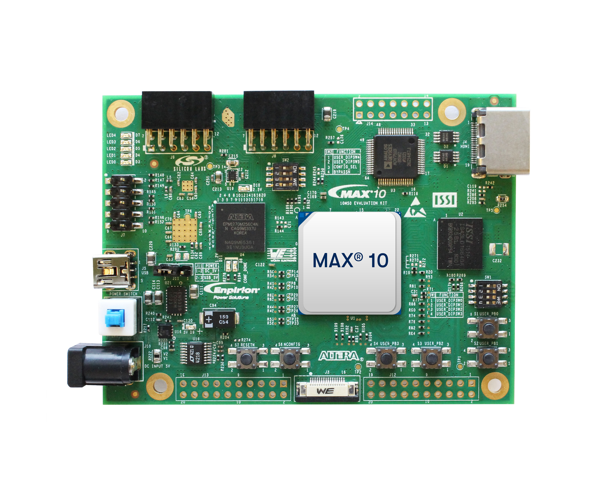
Figure 3: Intel MAX 10 FPGA Evaluation Kit — ideal for prototyping 10M16SAU169I7G application designs.
For rapid prototyping, Intel offers the MAX 10 FPGA Development Kit and the popular Terasic DE10-Lite board, both supported by the free Quartus Prime Lite Edition toolchain. Designers can also explore the 10M08SAE144C8G guide for a lower-density MAX 10 option in EQFP package.
Design Tutorial: Getting Started with MAX 10 FPGA
Video: Getting started with Intel MAX 10 FPGA development using Quartus Prime.
6. Frequently Asked Questions (FAQ)
Q1: What is the difference between 10M16SAU169I7G and 10M16SAU169C8G?
The I7G variant operates across the industrial temperature range (−40 °C to +100 °C) at speed grade 7, while the C8G variant covers the commercial range (0 °C to +85 °C) at speed grade 8. The I7G is recommended for harsh-environment and outdoor deployments where extended temperature resilience is required.
Q2: Does the 10M16SAU169I7G require an external configuration memory?
No. The MAX 10 family integrates on-chip configuration flash memory, enabling instant-on operation without any external PROM, EPCS, or serial flash. The device supports dual configuration images for safe remote updates.
Q3: How many ADC channels does the 10M16SAU169I7G provide?
The device includes a dual 12-bit ADC block capable of up to 1 MSPS sampling rate, with up to 18 analog input channels (depending on pin assignment). A dedicated temperature-sensing diode is also available on-chip.
Q4: What development tools are needed for the 10M16SAU169I7G?
The free Intel Quartus Prime Lite Edition fully supports all MAX 10 devices, including synthesis, place-and-route, timing analysis, and JTAG programming. No paid license is required. Programming is done via USB-Blaster or USB-Blaster II.
Q5: Can the 10M16SAU169I7G interface with DDR3 memory?
Yes. The MAX 10 family supports external memory interfaces including DDR3, DDR2, LPDDR2, and SRAM through its hard memory PHY. The 10M16 device in the U169 package provides up to 130 user I/O pins for memory and peripheral interfacing.
Q6: Where can I buy the 10M16SAU169I7G?
The 10M16SAU169I7G is available from authorized distributors and at wwdparts.com. Check stock availability and pricing on our website, or contact our sales team for volume quotes and lead-time information.


