
10M16SAU169I7G Datasheet, Specifications & Application Guide | Altera MAX 10 FPGA
The 10M16SAU169I7G is a non-volatile FPGA from the Altera (Intel) MAX 10 family, built on a 55 nm process node. Featuring 16,000 logic elements, an integrated dual 12-bit ADC, and internal flash configuration memory, this device delivers instant-on capability and mixed-signal integration in a compact 169-ball UBGA package. It is ideally suited for industrial control, IoT edge computing, motor drives, and sensor fusion applications where single-chip solutions reduce BOM cost and board space.
1. 10M16SAU169I7G Overview & Part Number Decoding
The 10M16SAU169I7G belongs to the Intel (formerly Altera) MAX 10 FPGA family — the industry's first single-chip, non-volatile FPGAs. Unlike traditional FPGAs that require external configuration flash, MAX 10 devices store their configuration internally, enabling instant-on operation within milliseconds of power-up.
Part Number Breakdown:
- 10M16 — MAX 10 family, 16,000 logic elements
- S — Single power-supply (no separate VCCIO bank voltage needed)
- A — Analog feature enabled (dual ADC block available)
- U169 — 169-ball Ultra Fine-pitch BGA package (11 mm × 11 mm)
- I — Industrial temperature grade (−40 °C to +100 °C)
- 7 — Speed grade 7 (fastest available for industrial temperature)
- G — Lead-free (RoHS compliant) packaging
2. Key Specifications & Parameters
| Parameter | Value |
|---|---|
| Device Family | Intel (Altera) MAX 10 |
| Logic Elements (LEs) | 16,000 |
| Logic Array Blocks (LABs) | 1,000 |
| Embedded Memory (M9K Blocks) | 549 Kbit |
| User Flash Memory (UFM) | 2,304 Kbit |
| 18 × 18 DSP Multipliers | 45 |
| Phase-Locked Loops (PLLs) | 4 |
| Maximum User I/O Pins | 130 |
| Analog-to-Digital Converter | Dual 12-bit, up to 1 MSPS |
| Package | 169-ball UBGA (11 mm × 11 mm, 0.8 mm pitch) |
| Core Voltage (VCC) | 1.2 V |
| I/O Voltage (VCCIO) | 3.3 V (single-supply mode) |
| Operating Temperature | −40 °C to +100 °C (Industrial) |
| Speed Grade | 7 (fastest industrial) |
| Process Technology | 55 nm |
| Configuration | Internal flash (instant-on), JTAG |
| LVDS Pairs | Up to 22 |
| External Memory Interface | DDR2, DDR3, LPDDR2, SRAM |
| RoHS Compliant | Yes |
3. Functional Block Diagram
The MAX 10 architecture integrates configurable logic blocks, embedded memory (M9K), DSP multipliers, PLLs, a dual ADC, and user flash memory on a single monolithic die. The diagram below illustrates the internal architecture of the MAX 10 family, including I/O banks, clock networks, and the integrated analog subsystem.

Key architectural highlights include:
- Instant-On Configuration: Dual-image internal flash eliminates external configuration devices and enables remote field updates.
- Integrated Dual ADC: Two 12-bit SAR ADCs with up to 18 analog input channels allow direct sensor interfacing without external ADC ICs.
- Flexible I/O: Supports LVTTL, LVCMOS (1.2 V–3.3 V), SSTL, HSTL, LVDS, and PCI standards.
- DSP Processing: 45 embedded 18 × 18 multipliers support FIR filters, FFTs, and signal-processing pipelines.
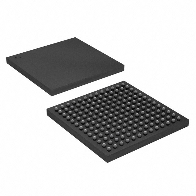
4. Package & Pinout Information
The 10M16SAU169I7G uses a 169-ball UBGA (Ultra Fine-pitch Ball Grid Array) package measuring 11 mm × 11 mm with 0.8 mm ball pitch. This compact form factor is ideal for space-constrained industrial and IoT designs. Of the 169 balls, 130 are available as user I/O, organized across multiple I/O banks supporting various voltage standards.
Pin-out files in PDF, XLS, and TXT formats are available from Altera's official pin-out resource page. For schematic symbol and PCB footprint, SnapEDA provides free downloadable CAD models compatible with Altium, KiCad, Eagle, and OrCAD.
5. Typical Application Circuits & Design Resources
The 10M16SAU169I7G excels in designs requiring instant-on FPGA logic combined with analog sensing. Common application areas include:
- Industrial Motor Control: Real-time PWM generation, encoder feedback processing, and current sensing via the integrated ADC.
- IoT Edge Gateways: Protocol bridging (SPI, I²C, UART), sensor data aggregation, and local inference acceleration.
- Medical Instrumentation: Multi-channel data acquisition, signal conditioning, and real-time waveform processing.
- Video Pre-Processing: Color-space conversion, frame buffering, and overlay generation for surveillance systems.
- Test & Measurement: High-speed data capture, pattern generation, and custom interface bridging.

For rapid prototyping, the MAX 10 FPGA Development Kit and the popular Terasic DE10-Lite board provide on-board USB-Blaster programming, SDRAM, VGA output, Arduino-compatible headers, and accelerometer sensors. Design examples and reference designs are available on Intel's GitHub repository.
Development Tools
All MAX 10 devices are supported by Intel Quartus Prime Lite Edition (free license), which includes synthesis, place-and-route, timing analysis, and the Platform Designer (Qsys) system integration tool. The Nios II soft-processor can be instantiated for embedded software development.
Video Tutorial
Watch this getting-started tutorial for the Altera/Intel MAX 10 development environment:
6. Frequently Asked Questions (FAQ)
Q1: What is the difference between 10M16SAU169I7G and 10M16SAU169C8G?
The primary differences are temperature grade and speed grade. The I7G variant supports the industrial temperature range (−40 °C to +100 °C) at speed grade 7, while the C8G variant is rated for commercial temperatures (0 °C to +85 °C) at speed grade 8. For harsh-environment or outdoor applications, the I7G is the appropriate choice.
Q2: Does the 10M16SAU169I7G require an external configuration flash?
No. MAX 10 FPGAs feature integrated configuration flash memory (CFM) that stores the FPGA bitstream internally. This enables instant-on operation — the device is fully configured within milliseconds of power-up, without any external flash or CPLD boot devices.
Q3: How many analog input channels does the dual ADC support?
The dual 12-bit ADC in the 10M16SAU169I7G supports up to 18 analog input channels (shared across both ADC cores), each capable of sampling at up to 1 MSPS. The ADC uses a successive-approximation register (SAR) architecture with a built-in temperature-sensing diode.
Q4: Can the 10M16SAU169I7G interface with DDR3 memory?
Yes. The MAX 10 family supports DDR3, DDR2, LPDDR2, and SRAM external memory interfaces. The hard memory controller IP facilitates integration with standard DDR3 SDRAM for applications requiring frame buffering, data logging, or processor-based systems with the Nios II soft core.
Q5: What design software is needed for the 10M16SAU169I7G?
Intel Quartus Prime Lite Edition is the recommended (and free) design tool. It supports RTL design entry in Verilog/VHDL/SystemVerilog, schematic capture, synthesis, place-and-route, timing analysis, and in-system debugging via SignalTap II. No paid license is required for MAX 10 devices.
Q6: Is the 10M16SAU169I7G suitable for safety-critical or automotive applications?
The I7G variant covers the industrial temperature range (−40 °C to +100 °C), which meets many industrial safety requirements. However, for automotive AEC-Q100 qualified parts, check Intel's automotive-grade MAX 10 offerings. The device supports SEU (Single Event Upset) mitigation through its configuration CRC error detection feature.


