
10M16SAU169I7G Datasheet, Specifications & Application Guide – Altera MAX 10 FPGA
The 10M16SAU169I7G is a non-volatile FPGA from the Altera (Intel) MAX 10 family, built on a 55 nm process node. Featuring 16,000 logic elements, an integrated dual 12-bit ADC, and internal flash configuration memory, it delivers instant-on operation ideal for industrial control, IoT edge computing, and mixed-signal embedded systems. This comprehensive guide covers the 10M16SAU169I7G datasheet highlights, pinout, key electrical parameters, and practical design considerations.
1. 10M16SAU169I7G Overview & Part Number Decoding
The 10M16SAU169I7G belongs to the Intel (Altera) MAX 10 FPGA family — a single-chip, non-volatile FPGA platform that eliminates the need for external configuration flash. The part number decodes as follows:
- 10M16 – MAX 10 device with 16,000 logic elements
- S – Single power-supply (integrated 1.2 V core regulator)
- A – Analog block enabled (dual 12-bit ADC)
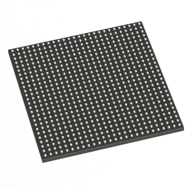
- U169 – 169-ball UBGA package (11 mm × 11 mm)
- I – Industrial temperature range (−40 °C to +100 °C)
- 7 – Speed grade 7 (highest performance tier)
- G – Lead-free (RoHS compliant)
Unlike SRAM-based FPGAs that require external configuration flash or EEPROM, the MAX 10 stores its bitstream in on-chip flash memory, enabling instant-on operation within milliseconds of power-up. This makes the 10M16SAU169I7G especially attractive for safety-critical and latency-sensitive applications.
2. Key Specifications & Electrical Parameters
| Parameter | Value |
|---|---|
| Logic Elements (LEs) | 16,000 |
| Embedded Memory (M9K RAM) | 549 Kb |
| User Flash Memory (UFM) | 2,304 Kb |
| 18 × 18 Multiplier DSP Blocks | 45 |
| PLLs | 4 |
| Maximum User I/O Pins | 130 (U169 package) |
| ADC | Dual 12-bit, up to 1 MSPS, 18 analog input channels |
| Core Voltage | 1.2 V (internally regulated) |
| I/O Supply Voltage | 3.0 V / 3.3 V |
| I/O Standards Supported | LVTTL, LVCMOS, SSTL, HSTL, LVDS, TMDS |
| External Memory Interfaces | DDR2, DDR3, LPDDR2, SRAM |
| Package | 169-ball UBGA (11 mm × 11 mm, 0.8 mm pitch) |
| Operating Temperature | −40 °C to +100 °C (Industrial) |
| Process Technology | 55 nm |
| Configuration | Internal flash, dual-image boot supported |
| FPGA Bitstream Security | AES-128 encryption |
3. Functional Block Diagram
The MAX 10 architecture integrates logic array blocks (LABs), M9K embedded memory, DSP multiplier blocks, PLLs, a dual ADC, and user flash memory into a column-based fabric. The diagram below illustrates the internal architecture of Intel MAX 10 FPGA devices:

Key architectural highlights include:
- Logic Array Blocks (LABs) – Each LAB contains 16 LEs with four-input LUTs and programmable registers
- M9K Memory Blocks – 9,216-bit SRAM blocks configurable as RAM, ROM, shift registers, or FIFO
- DSP Blocks – 45 embedded 18 × 18 multipliers for signal processing pipelines
- Dual 12-bit ADC – Up to 1 MSPS with internal temperature sensor and voltage reference
- Configuration Flash – On-chip non-volatile storage supporting dual-image boot and remote system update
4. Pinout & Package Information
The 10M16SAU169I7G is housed in a compact 169-ball UBGA package measuring 11 mm × 11 mm with 0.8 mm ball pitch. The U169 package provides 130 user I/O pins organized across multiple I/O banks supporting a wide range of voltage standards.
The package supports up to 22 LVDS differential pairs and provides dedicated pins for JTAG programming, ADC analog inputs, and PLL reference clocks. Pin-out files in PDF, XLS, and TXT formats are available from Altera's pin-out resource page. Schematic symbols and PCB footprints can be downloaded from SnapEDA.
5. Typical Applications & Design Resources
The 10M16SAU169I7G is widely deployed across a range of embedded and industrial applications:
- Industrial Control & Motor Drives – Real-time PWM generation, encoder interfaces, and sensor fusion leveraging the integrated ADC
- IoT Edge Gateways – Protocol bridging (SPI, I²C, UART, Ethernet), data aggregation, and hardware-accelerated encryption
- Video Surveillance Pre-Processing – Low-latency image scaling, color-space conversion, and overlay generation
- Medical Instrumentation – Analog front-end digitization with the on-chip ADC, signal conditioning, and digital filtering
- Automotive Sensor Hubs – Instant-on operation for functional-safety applications requiring fast boot times

Altera provides the MAX 10 FPGA Development Kit and the popular Terasic DE10-Lite board for rapid prototyping. Both include USB-Blaster programming, SDRAM, VGA output, and Arduino-compatible expansion headers. The free Quartus Prime Lite Edition provides full synthesis, place-and-route, and JTAG programming support for all MAX 10 devices.
Video Tutorial: Getting Started with Intel MAX 10 FPGA
For more FPGA and semiconductor resources, explore these guides on WWDParts:
- 10M08SAE144C8G – Intel MAX 10 FPGA Datasheet & Application Guide
- 10M16SAU169C8G – Intel MAX 10 FPGA Specifications & Pinout
- WWDParts Semiconductor Blog – Latest Datasheets & Guides
6. FAQ – 10M16SAU169I7G
What is the difference between the 10M16SAU169I7G and 10M16SAU169C8G?
The main differences are temperature range and speed grade. The I7G variant supports the industrial temperature range (−40 °C to +100 °C) with speed grade 7 (fastest), while the C8G variant is rated for commercial temperature (0 °C to +85 °C) with speed grade 8 (slower). The I7G is preferred for harsh-environment and industrial applications.
Does the 10M16SAU169I7G require external configuration memory?
No. The MAX 10 family features internal flash configuration memory, eliminating the need for external SPI flash or EEPROM. The device stores its bitstream on-chip and boots instantly within milliseconds of power-up. It also supports dual-image boot for safe remote firmware updates.
What development tools are needed to program the 10M16SAU169I7G?
You need the Quartus Prime Lite Edition (free download from Intel/Altera), which includes synthesis, place-and-route, timing analysis, and the JTAG programmer. A USB-Blaster or USB-Blaster II cable is used for JTAG programming. For simulation, ModelSim-Intel Starter Edition is included at no cost.
How many ADC channels does the 10M16SAU169I7G have?
The 10M16SAU169I7G integrates a dual 12-bit ADC capable of sampling at up to 1 MSPS. It supports up to 18 single-ended analog input channels, plus an internal temperature sensor and on-chip voltage reference — making it ideal for mixed-signal designs without requiring external ADC ICs.
What is the maximum operating frequency of the 10M16SAU169I7G?
The speed grade 7 designation indicates the fastest performance tier in the MAX 10 family. The four integrated PLLs support clock management up to 500 MHz. Actual operating frequency for user logic depends on design complexity and timing closure in Quartus Prime.
Can the 10M16SAU169I7G interface with DDR3 memory?
Yes. The MAX 10 family supports DDR2, DDR3, LPDDR2, and SRAM external memory interfaces through dedicated I/O pins with DQS-based capture. However, the U169 package has a limited pin count (130 I/O), so designers should verify sufficient pins are available for the desired memory bus width plus other peripherals.


