
10M16SAU169I7G Datasheet, Specifications & Application Guide – Altera MAX 10 FPGA
1. Overview of the 10M16SAU169I7G
The 10M16SAU169I7G is a non-volatile FPGA from the Intel (Altera) MAX 10 family, fabricated on a 55 nm flash process. It combines 16,000 logic elements with an integrated dual 12-bit ADC, embedded SRAM, user flash memory, and instant-on capability — all in a compact 169-ball UBGA package rated for industrial temperatures (−40 °C to +100 °C).
The MAX 10 family eliminates the need for external configuration devices by storing the bitstream in on-chip flash. This makes the 10M16SAU169I7G an ideal single-chip solution for industrial control, motor drives, sensor fusion, IoT edge gateways, video pre-processing, and medical instrumentation. Its single-supply operation (denoted by the "S" in the part number) simplifies board design and reduces BOM cost.
Looking for similar MAX 10 devices? Check out the 10M16SAU169C8G (commercial grade) or the 10M08SAE144C8G (8K LE variant in EQFP-144).
2. Key Specifications & Parameters
| Parameter | Value |
|---|---|
| Part Number | 10M16SAU169I7G |
| Family | Intel (Altera) MAX 10 |
| Process Technology | 55 nm Flash |
| Logic Elements (LEs) | 16,000 |
| Logic Array Blocks (LABs) | 1,000 |
| Embedded SRAM (M9K) | 549 Kb |
| User Flash Memory (UFM) | 2,304 Kb |
| DSP Blocks (18×18 Multipliers) | 45 |
| Analog-to-Digital Converter | Dual 12-bit ADC (1 MSPS) |
| Maximum I/O Pins | 130 |
| Package | 169-ball UBGA (11 × 11 mm) |
| Core Voltage | 1.2 V |
| I/O Standards | 3.3 V, 2.5 V, 1.8 V, 1.5 V LVCMOS/LVTTL; LVDS |
| Operating Temperature | −40 °C to +100 °C (Industrial) |
| Speed Grade | 7 |
| Configuration | Internal Flash (Instant-On), JTAG |
| Power Supply | Single-Supply Operation |
| RoHS Compliant | Yes (Lead-Free / Green) |
3. Block Diagram & Architecture
The MAX 10 architecture centers on adaptive logic modules (ALMs) organized into LABs, flanked by embedded memory blocks, DSP slices, and a dual-channel ADC. The internal flash configuration memory enables instant-on operation and dual boot images for fail-safe field updates.
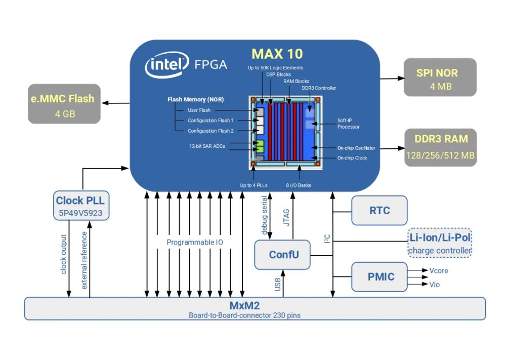
Figure 1: Intel MAX 10 FPGA internal block diagram – logic fabric, embedded memory, DSP, and ADC subsystem.
4. Pinout & Package Information
The 10M16SAU169I7G uses a 169-ball UBGA package (11 × 11 mm, 0.8 mm ball pitch) with 130 user I/O pins. The compact form factor supports high-density PCB designs while providing ample I/O for typical industrial and IoT applications. Multi-voltage I/O banks allow interfacing with 3.3 V, 2.5 V, 1.8 V, and 1.5 V logic levels.
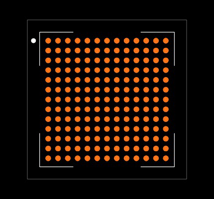
Figure 2: 10M16SAU169I7G UBGA-169 package footprint (courtesy of SnapEDA).
5. Application Circuit & Design Resources
A typical MAX 10 application circuit includes the FPGA, decoupling capacitors on each power rail, a 50 MHz oscillator, JTAG header, and level-shifting buffers for mixed-voltage interfaces. The integrated ADC simplifies analog sensor front-ends by eliminating external ADC ICs. For rapid prototyping, the official MAX 10 FPGA Development Kit and the popular Terasic DE10-Lite board provide USB-Blaster programming, SDRAM, VGA, Arduino headers, and an accelerometer.
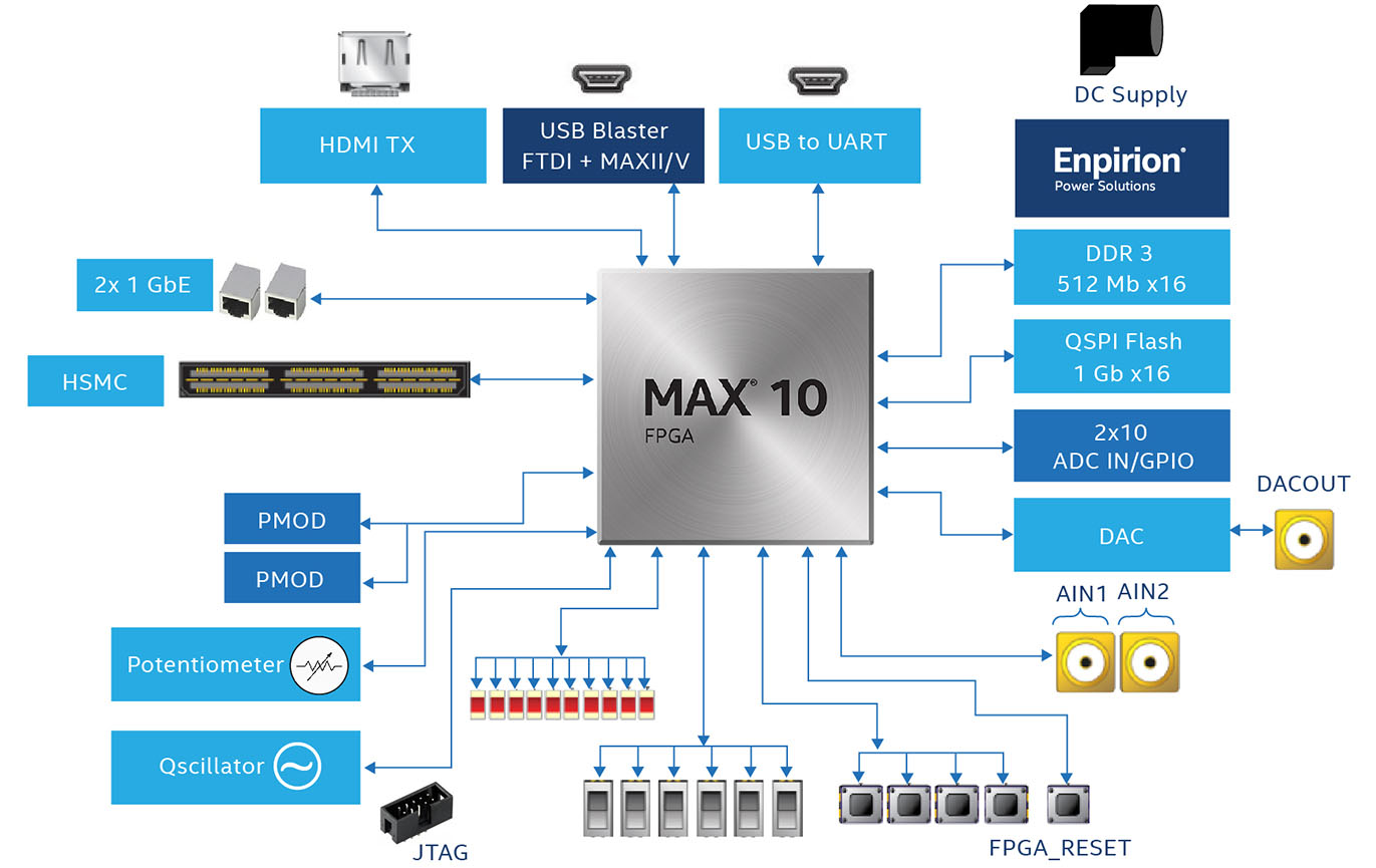
Figure 3: MAX 10 FPGA Development Kit block diagram – typical application connections.
Design tools: Download Quartus Prime Lite Edition (free) from Intel for synthesis, place-and-route, timing analysis, and JTAG programming. The 10M16SAU169C8G guide covers shared PCB layout recommendations.
Video Tutorial: Getting Started with MAX 10 FPGA
6. FAQ – Frequently Asked Questions
Q1: What is the difference between 10M16SAU169I7G and 10M16SAU169C8G?
The I7G variant is rated for the industrial temperature range (−40 °C to +100 °C) with speed grade 7, while the C8G is a commercial-grade part (0 °C to +85 °C) with speed grade 8. The "I" suffix indicates industrial and the "C" indicates commercial. Choose the I7G for applications exposed to extreme temperatures such as outdoor industrial equipment or automotive-adjacent systems.
Q2: Does the 10M16SAU169I7G require an external configuration flash?
No. MAX 10 FPGAs store their configuration bitstream in on-chip flash memory, enabling instant-on operation without any external configuration device (EPCQ, etc.). The device supports dual configuration images for fail-safe remote updates.
Q3: How many ADC channels does the 10M16SAU169I7G have?
The device integrates a dual 12-bit ADC with up to 18 analog input channels (shared with I/O pins) and a maximum sampling rate of 1 MSPS per ADC block. This is sufficient for temperature sensors, current monitors, and general-purpose analog measurements in industrial applications.
Q4: What development board supports the 10M16SAU169I7G?
While the exact U169 package variant is not on a mainstream dev board, the Terasic DE10-Lite (10M50DAF484) and the Arrow MAX1000 (10M08SAU169) use the same MAX 10 architecture and are pin-compatible in many design aspects. Code and IP developed on these boards can be directly ported to the 10M16SAU169I7G with minimal changes.
Q5: What is the maximum operating frequency of the 10M16SAU169I7G?
The speed grade 7 variant supports register-to-register performance up to approximately 300 MHz for simple logic paths. Actual achievable frequency depends on design complexity, routing congestion, and timing constraints. Use Quartus Prime's TimeQuest Timing Analyzer for accurate timing closure.
Q6: Can I use LVDS I/O with the 10M16SAU169I7G?
Yes. The MAX 10 family supports LVDS (Low-Voltage Differential Signaling) on dedicated I/O pairs, enabling high-speed serial interfaces up to 875 Mbps. The U169 package provides several LVDS-capable pin pairs — consult the Intel pin-out file for exact locations.


