
10M16SAU169I7G Datasheet, Pinout, Specifications & Application Guide | Altera MAX 10 FPGA
The 10M16SAU169I7G is an Altera (Intel) MAX 10 non-volatile FPGA delivering 16,000 logic elements, an integrated dual 12-bit ADC, and on-chip configuration flash in a compact 169-ball UBGA package. Built on 55nm flash-based process technology with industrial-grade temperature support (−40°C to +100°C), the "SA" single-supply variant simplifies power design for harsh-environment applications. This comprehensive guide covers the 10M16SAU169I7G pinout, datasheet specifications, block diagram, and typical application circuits to accelerate your next embedded FPGA design.
Overview & Key Features
The 10M16SAU169I7G belongs to the Altera MAX 10 FPGA family, the industry's first single-chip non-volatile FPGA to combine flash-based configuration, analog-to-digital conversion, and flexible I/O in one device. Unlike SRAM-based FPGAs that require external configuration memory, the MAX 10 stores its bitstream in on-chip dual configuration flash, enabling instant-on operation within milliseconds of power-up.
Key features of the 10M16SAU169I7G include:
- 16,000 Logic Elements (LEs) — organized in 1,000 Logic Array Blocks (LABs), providing ample capacity for complex state machines, protocol bridges, and digital signal processing
- Dual 12-bit ADC — two independent ADC blocks with up to 1 MSPS sampling rate, eliminating external ADC components in mixed-signal designs
- 549 Kb Embedded RAM — M9K memory blocks for FIFO buffers, lookup tables, and on-chip data storage
- 2,304 Kb User Flash Memory — on-chip non-volatile storage for calibration data, firmware, or boot parameters
- 45 DSP Multipliers — 18×18 embedded multipliers for efficient digital filtering and arithmetic operations
- 130 User I/O Pins — supporting 3.3V LVTTL, 1.0–3.3V LVCMOS, SSTL, HSTL, and LVDS standards
- Single 3.3V Supply — internal voltage regulators generate the 1.2V core supply (SA variant), simplifying board-level power design
- Industrial Temperature Range — −40°C to +100°C operation for automotive, industrial, and outdoor deployments
- Instant-On Operation — non-volatile configuration eliminates external boot flash and reduces system startup latency
The MAX 10 family is fully supported by Intel Quartus Prime Lite Edition, a free-of-charge development environment providing synthesis, place-and-route, timing analysis, and JTAG/in-system programming.
Technical Specifications
| Parameter | Value |
|---|---|
| Manufacturer | Altera (Intel) |
| Family | MAX 10 FPGA |
| Part Number | 10M16SAU169I7G |
| Logic Elements (LEs) | 16,000 |
| Logic Array Blocks (LABs) | 1,000 |
| Embedded Memory (M9K) | 549 Kb |
| User Flash Memory (UFM) | 2,304 Kb |
| 18×18 Multipliers | 45 |
| PLLs | 2 |
| ADC Blocks | 2 (dual 12-bit, 1 MSPS) |
| Maximum User I/O Pins | 130 |
| I/O Standards | 3.3V LVTTL, 1.0–3.3V LVCMOS, SSTL, HSTL, LVDS |
| Package | 169-ball UBGA (Ultra-thin Ball Grid Array) |
| Package Dimensions | 11 mm × 11 mm, 0.8 mm pitch |
| Core Voltage (VCCINT) | 1.2V (internally regulated) |
| I/O Voltage (VCCIO) | 1.2V / 1.5V / 1.8V / 2.5V / 3.3V (bank-selectable) |
| Supply Voltage | 3.0V / 3.3V single supply (SA variant) |
| Process Technology | 55 nm Flash |
| Speed Grade | 7 (industrial) |
| Temperature Range | −40°C to +100°C (industrial) |
| Configuration | Dual-image internal flash, JTAG |
| RoHS Compliant | Yes (Pb-free, "G" suffix) |
Pinout & Package Information
The 10M16SAU169I7G is housed in a 169-ball Ultra-thin Ball Grid Array (UBGA) package measuring 11 mm × 11 mm with 0.8 mm ball pitch. The compact UBGA form factor makes it well-suited for space-constrained designs in IoT edge devices, wearable electronics, and small-form-factor industrial modules. The 130 user I/O pins are organized across multiple I/O banks, each independently configurable for different voltage standards.

Pin Categories:
- VCCINT — 1.2V core supply (internally regulated in SA single-supply variant)
- VCCIO — I/O bank supply voltage (3.3V typical, bank-selectable from 1.2V to 3.3V)
- VCCA / VCCD_PLL — PLL analog and digital supply pins
- VREFB — voltage reference for I/O banks supporting referenced I/O standards
- ANAIN — dedicated analog input pins for the integrated dual 12-bit ADC
- CLK[0..3] — dedicated clock input pins routed to global clock networks and PLLs
- JTAG (TCK, TMS, TDI, TDO) — programming, debug, and boundary-scan interface
- nSTATUS, nCONFIG, CONF_DONE — configuration status and control pins
For the complete pinout table and I/O bank assignments, refer to the official 10M16SAU169I7G product page or the Intel MAX 10 Pin-Out Files available from the Altera website.
Block Diagram & Architecture
The MAX 10 architecture combines a traditional FPGA logic fabric with embedded flash, analog, and memory blocks in a single die. The 10M16SAU169I7G's internal architecture is organized around a grid of 1,000 LABs (each containing 16 adaptive logic modules), surrounded by M9K embedded memory blocks, DSP multiplier blocks, PLLs, and I/O elements.

Architecture Highlights:
- Adaptive Logic Modules (ALMs) — each LAB contains 16 logic elements with 4-input LUTs, carry chains, and register packing for maximum logic density
- M9K Memory Blocks — 9 Kb dual-port SRAM blocks configurable as single-port RAM, dual-port RAM, ROM, or FIFO, providing 549 Kb total embedded memory
- DSP Blocks — 45 embedded 18×18 multipliers supporting multiply-accumulate operations for FIR filters, FFTs, and matrix computations
- Dual ADC — two 12-bit successive-approximation ADCs with internal voltage reference and temperature sensor, controlled via an Avalon-MM slave interface
- Configuration Flash Memory (CFM) — dual-image storage enabling remote field updates with automatic fallback to a known-good image
- User Flash Memory (UFM) — 2,304 Kb non-volatile storage accessible through an Avalon-MM interface for application data
- Global Clock Networks — 2 PLLs with up to 5 output clocks each, plus 4 dedicated clock input pins for low-jitter clock distribution
Application Circuit & Design Guide
The 10M16SAU169I7G's combination of instant-on FPGA logic, integrated ADC, and industrial-grade temperature range makes it an excellent fit for a wide range of embedded applications. Below are typical use cases and design considerations.
Typical Applications:
- Industrial Sensor Hub — use the dual ADC to digitize multiple analog sensors (temperature, pressure, current) while the FPGA fabric handles real-time signal conditioning, threshold detection, and communication protocol conversion (SPI/I2C to Ethernet or CAN)
- Motor Drive Controller — implement space-vector PWM generation, encoder interface, and closed-loop PID control in a single chip with deterministic sub-microsecond latency
- IoT Edge Gateway — combine protocol bridging (Modbus RTU to MQTT), local data preprocessing, and secure boot capabilities using the dual configuration flash for over-the-air updates
- Video Pre-Processing — perform pixel-level operations such as de-Bayering, noise reduction, and frame buffering for CMOS image sensors before passing data to a host processor
- Medical Instrumentation — leverage the ADC for biopotential acquisition (ECG, EMG) with the FPGA fabric implementing digital filtering and data packetization
Power Supply Design Tips:
- The SA variant requires only a single 3.3V supply — connect VCC_ONE to 3.3V and the internal LDOs generate VCCINT (1.2V)
- Place 0.1 µF decoupling capacitors on each VCC and VCCIO ball; add a 10 µF bulk capacitor per power rail
- Route analog supply (VCCA_ADC) through a ferrite bead and separate ground pour to minimize digital noise coupling into the ADC
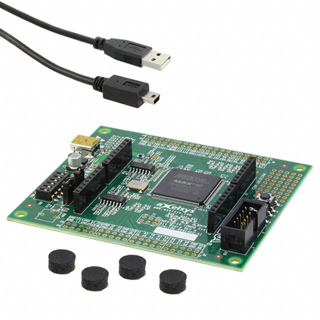
For development and rapid prototyping, Altera offers the MAX 10 FPGA Evaluation Kit and the popular Terasic DE10-Lite board, both supporting the MAX 10 device family with on-board USB-Blaster programming, SDRAM, and expansion headers.
Frequently Asked Questions
What is the difference between 10M16SAU169I7G and 10M16SAU169C8G?
The key differences are temperature range and speed grade. The 10M16SAU169I7G is an industrial-grade device rated for −40°C to +100°C with speed grade 7, while the 10M16SAU169C8G is a commercial-grade device rated for 0°C to 85°C with speed grade 8. Both share the same 16,000 LE logic fabric, dual ADC, and 169-ball UBGA package. Choose the "I7G" variant for applications requiring extended temperature operation such as outdoor industrial equipment or automotive subsystems.
Does the 10M16SAU169I7G require an external configuration flash?
No. The MAX 10 FPGA family includes on-chip dual configuration flash memory, so no external configuration PROM or SPI flash is needed. The device stores up to two configuration images internally, enabling instant-on power-up (typically under 10 ms) and supporting remote firmware updates with automatic fallback to a known-good image if the primary image fails integrity checks.
What development tools are needed to program the 10M16SAU169I7G?
You need Intel Quartus Prime Lite Edition (free download), which provides full support for all MAX 10 devices including synthesis, place-and-route, timing analysis, and SignalTap logic analyzer. For programming, use a USB-Blaster or USB-Blaster II cable connected to the JTAG pins. The Quartus suite also includes the Nios II Embedded Design Suite for implementing soft processor systems and the Platform Designer (Qsys) tool for system integration.
How do I use the integrated ADC on the 10M16SAU169I7G?
The dual 12-bit ADC blocks are accessed through an Avalon Memory-Mapped (Avalon-MM) slave interface. In Quartus, instantiate the "Altera Modular ADC" IP core via Platform Designer, configure the number of channels and sampling rate, and connect it to a Nios II processor or custom logic via the Avalon bus. Each ADC supports up to 1 MSPS sampling with an internal 2.5V reference. Dedicated analog input pins (ANAIN) should be routed with short traces away from high-speed digital signals for optimal noise performance.
Can the 10M16SAU169I7G run a soft processor?
Yes. The 16,000 LEs provide sufficient resources to implement a Nios II/e (economy) or Nios II/f (fast) soft processor with peripherals such as UART, SPI, I2C, timers, and GPIO. A typical Nios II/e system consumes approximately 600–800 LEs, leaving ample capacity for custom hardware accelerators alongside the processor. This enables a complete system-on-chip design without an external microcontroller.
What is the maximum operating frequency of the 10M16SAU169I7G?
The speed grade 7 designation indicates the slowest speed bin in the MAX 10 family. Typical Fmax values depend on design complexity: simple register-to-register paths can achieve 250–300 MHz, while complex designs with significant routing utilization typically operate at 100–180 MHz. The two on-chip PLLs support output frequencies from 4.69 MHz to 472.5 MHz, enabling flexible clock synthesis for various interface standards and processing requirements.


