
10M16SAU169I7G Datasheet, Specifications & Application Guide – Altera MAX 10 FPGA
1. Overview of the 10M16SAU169I7G
The 10M16SAU169I7G is a non-volatile FPGA from the Altera (Intel) MAX 10 family, fabricated on a 55 nm flash process. It delivers 16,000 logic elements with an integrated dual 12-bit ADC, internal configuration flash, and instant-on capability—eliminating the need for an external configuration device. This makes it ideal for cost-sensitive, space-constrained embedded applications in industrial automation, motor control, IoT edge computing, and medical instrumentation.
The part number decodes as: 10M16 (MAX 10, 16K LEs) + S (single supply) + A (analog/ADC enabled) + U169 (169-ball UBGA) + I (industrial temp −40°C to +100°C) + 7 (speed grade 7).
Whether you are prototyping a sensor-fusion hub or deploying a rugged fieldbus interface, the 10M16SAU169I7G offers the right balance of logic density, analog integration, and power efficiency. You can source the 10M16SAU169I7G at WWDParts with competitive pricing and fast shipping.
2. Key Specifications & Parameters
| Parameter | Value |
|---|---|
| Manufacturer | Altera (Intel) |
| Family | MAX 10 (10M16) |
| Process Node | 55 nm Flash |
| Logic Elements (LEs) | 16,000 |
| Logic Array Blocks (LABs) | 1,000 |
| Embedded Memory (M9K) | 549 Kb |
| User Flash Memory (UFM) | 2,304 Kb |
| 18×18 DSP Multipliers | 45 |
| ADC | Dual 12-bit, up to 1 MSPS |
| Maximum User I/O | 130 |
| Package | 169-ball UBGA (11 × 11 mm) |
| Supply Voltage (VCCINT) | 3.0 V – 3.3 V (single supply) |
| Operating Temperature | −40 °C to +100 °C (Industrial) |
| Speed Grade | 7 |
| Configuration | Internal flash – instant-on |
| PLL | Up to 2 |
| Global Clock Networks | Up to 20 |
3. Block Diagram & Internal Architecture
The MAX 10 architecture integrates logic elements, embedded memory blocks, DSP blocks, a dual ADC, user flash memory, and PLLs within a single die. The block diagram below illustrates the internal interconnect and peripheral placement of a MAX 10 development system.
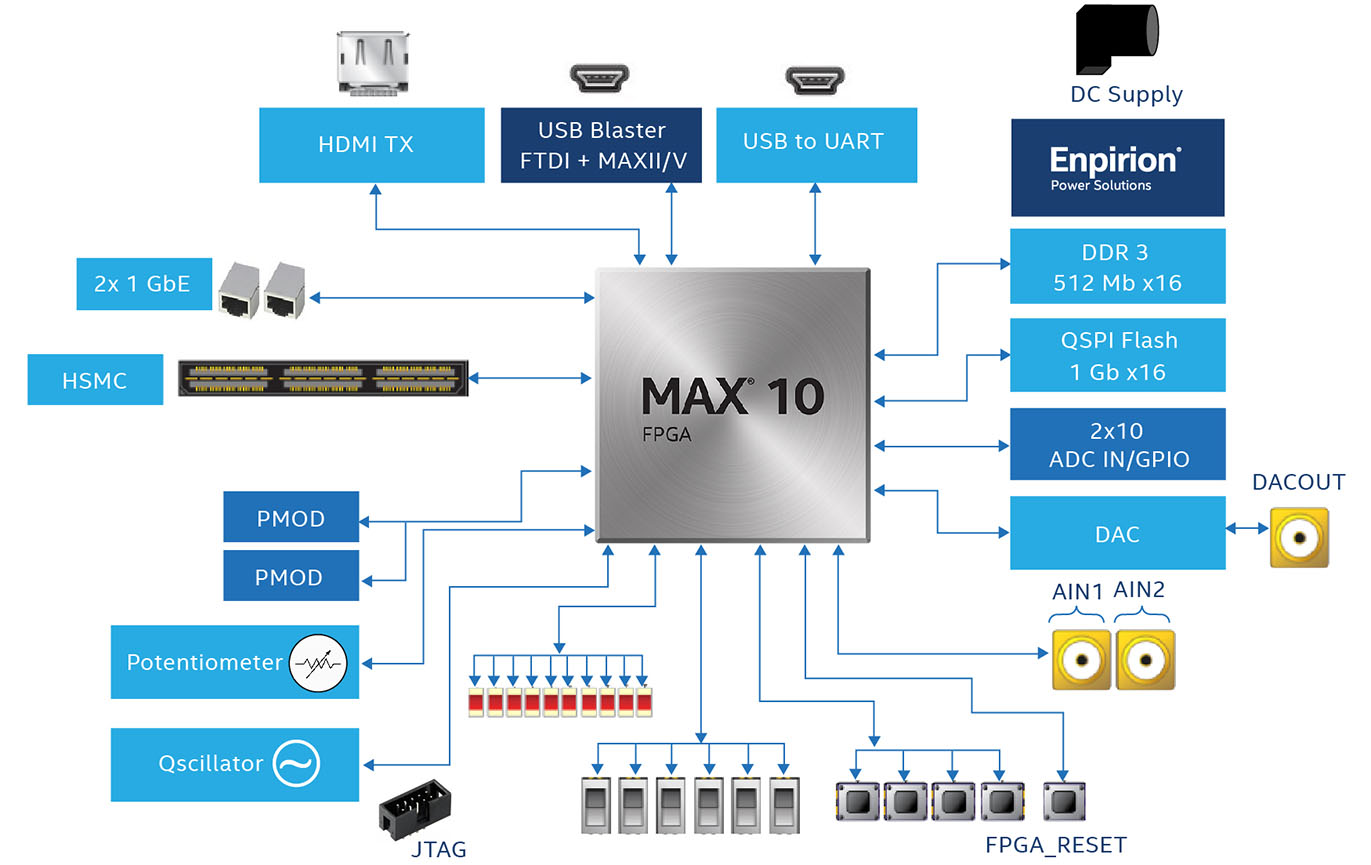
Key architectural highlights include the dual 12-bit ADC with up to 18 analog input channels, 45 embedded 18×18 multipliers for DSP-intensive workloads, and dual configuration images stored in on-chip flash for remote update with safe fallback.
4. Pinout, Package & Thermal Information
The 10M16SAU169I7G ships in a 169-ball UBGA package measuring 11 × 11 mm with a 0.8 mm ball pitch. It provides up to 130 user I/O pins organized into multiple I/O banks supporting 3.3 V, 2.5 V, 1.8 V, and 1.5 V LVTTL/LVCMOS standards, as well as LVDS differential signaling on select banks.

Thermal management is straightforward thanks to the low static power of the 55 nm process. Typical junction-to-ambient thermal resistance (θJA) for the UBGA-169 is approximately 25 °C/W, allowing fanless operation in most industrial enclosures. For designs pushing the full 16K LE utilization at speed grade 7, a simple copper pour under the package is recommended.
5. Application Circuit & Design Guide
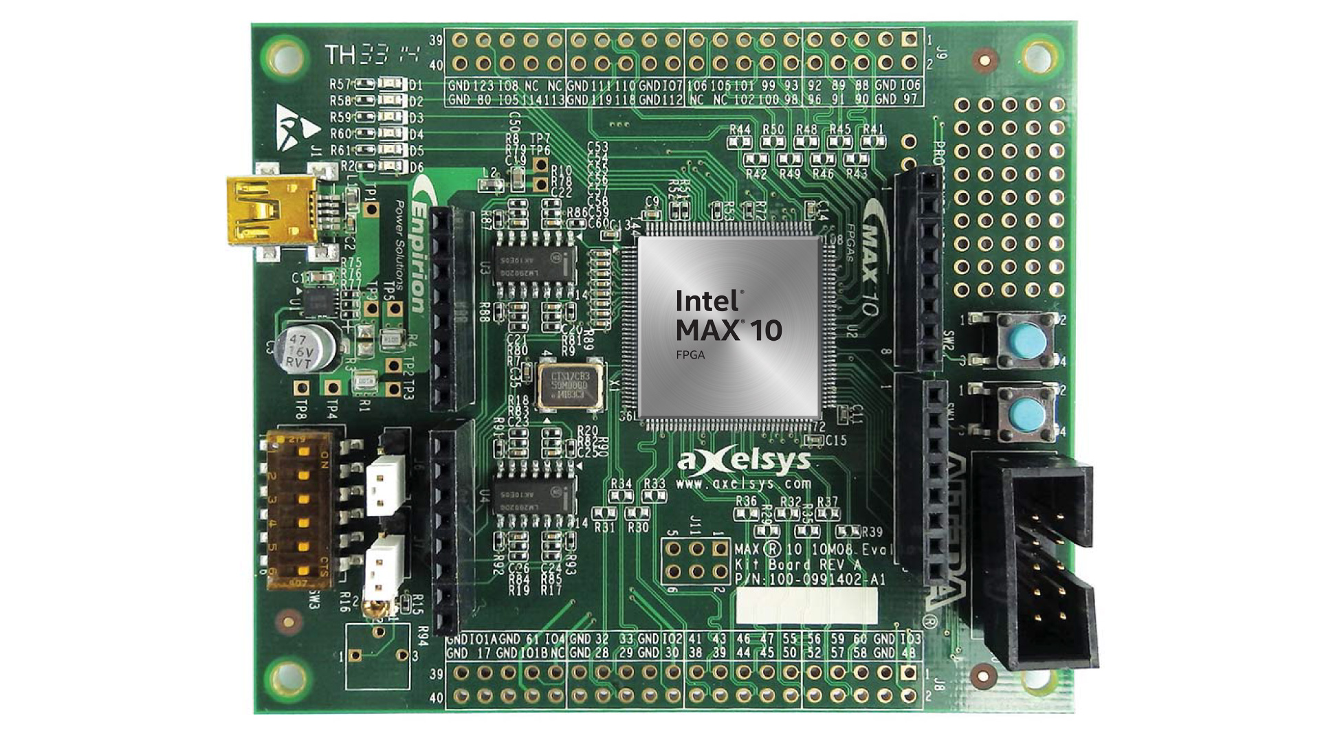
The 10M16SAU169I7G excels in mixed-signal embedded designs where analog sensing and digital processing must coexist on a single chip. Below is the MAX 10 FPGA Evaluation Board—a reference design commonly used for rapid prototyping with the 10M16 device.
Design Tips
- Power Supply: Use a single 3.3 V rail with adequate decoupling (100 nF per VCC pin + 10 µF bulk). The single-supply variant (S) simplifies board design.
- Configuration: Internal flash stores two configuration images—use dual-image mode for safe remote firmware updates via JTAG or embedded Nios II soft processor.
- ADC Integration: Route analog inputs with proper ground isolation and series resistors. The on-chip ADC supports up to 1 MSPS per channel.
- Development Tools: Quartus Prime Lite Edition (free) supports all MAX 10 devices including synthesis, place-and-route, timing analysis, and JTAG programming.
Video Tutorial: Getting Started with Intel MAX 10 FPGA
6. Frequently Asked Questions (FAQ)
Q1: What is the 10M16SAU169I7G and which family does it belong to?
The 10M16SAU169I7G is a non-volatile FPGA from the Intel (Altera) MAX 10 family. It offers 16,000 logic elements, a dual 12-bit ADC, and on-chip flash configuration in a compact 169-ball UBGA package, designed for industrial-temperature operation from −40 °C to +100 °C.
Q2: Does the 10M16SAU169I7G require an external configuration memory?
No. The MAX 10 family features internal flash-based configuration, providing instant-on operation without an external EEPROM or serial flash. It supports dual configuration images for remote update with safe fallback.
Q3: What is the operating voltage of the 10M16SAU169I7G?
The device operates from a single 3.0 V to 3.3 V supply (VCCINT). The "S" in the part number indicates single-supply operation, simplifying power delivery and reducing BOM cost.
Q4: How many I/O pins are available on the 10M16SAU169I7G?
The UBGA-169 package provides up to 130 user I/O pins supporting multiple voltage standards (3.3 V, 2.5 V, 1.8 V, 1.5 V LVTTL/LVCMOS) and select LVDS pairs.
Q5: What development tools are needed for the 10M16SAU169I7G?
Intel's Quartus Prime Lite Edition (free, no license required) provides full design flow support including RTL synthesis, place-and-route, timing analysis, and JTAG/AS programming. The DE10-Lite and MAX 10 Evaluation Kit are popular starter boards.
Q6: Where can I buy the 10M16SAU169I7G at competitive pricing?
You can purchase the 10M16SAU169I7G with guaranteed authenticity and fast global shipping at WWDParts.com. We offer flexible quantities for both prototyping and volume production.


