
10M16SAU169I7G Datasheet, Pinout, Specs & Application Guide — Altera MAX 10 FPGA
The 10M16SAU169I7G is a non-volatile FPGA from the Altera (Intel) MAX 10 family, built on 55 nm flash process technology. With 16,000 logic elements, an integrated 12-bit ADC, on-chip user flash memory, and instant-on capability, it targets industrial control, sensor fusion, motor drives, and IoT edge applications where a single-chip programmable solution eliminates external configuration devices and reduces board area. This guide covers the full datasheet specifications, pinout, block diagram, typical application circuits, and design resources for the 10M16SAU169I7G.
1. Device Overview & Part Number Decoding
The MAX 10 family is Altera's first non-volatile FPGA product line, combining programmable logic with on-die flash storage, a 12-bit analog-to-digital converter, and support for the Nios II embedded processor — all in a single chip. The 10M16SAU169I7G part number decodes as follows:
- 10M16 — MAX 10 family, 16,000 logic elements
- S — Single-supply device (internal voltage regulator, no external 1.2 V core rail required)
- A — Analog feature enabled (integrated ADC block)
- U169 — UBGA-169 package (169-ball Ultra Fine-pitch BGA, 11 × 11 mm)
- I7 — Industrial temperature range (−40 °C to +100 °C), speed grade 7
- G — Lead-free (RoHS compliant) packaging
Compared to traditional FPGA families that require external serial flash for configuration, the MAX 10 stores its bitstream in on-chip flash, enabling instant-on operation within milliseconds of power-up. This architecture supports dual boot images for safe remote field updates. For more single-supply Altera MAX 10 options, see our guides on the 10M16SAU169C8G (commercial variant) and the 10M08SAE144C8G (8K LE variant).
2. Key Specifications & Electrical Parameters
| Parameter | Value |
|---|---|
| Family | Altera MAX 10 (10M16) |
| Logic Elements (LEs) | 16,000 |
| Logic Array Blocks (LABs) | 1,000 |
| Embedded Memory (M9K blocks) | 549 Kbit |
| User Flash Memory (UFM) | 2,304 Kbit |
| 18 × 18 Embedded Multipliers | 45 |
| Phase-Locked Loops (PLLs) | 4 |
| Global Clock Networks | 20 |
| Maximum User I/O Pins | 130 (U169 package) |
| Maximum LVDS Pairs | 22 |
| ADC Channels | Dual 12-bit, up to 1 MSPS, 17 analog inputs |
| Package | UBGA-169 (11 × 11 mm, 0.8 mm pitch) |
| Core Voltage | 1.2 V (internally regulated from 3.0 V / 3.3 V supply) |
| I/O Voltage | 1.2 V, 1.5 V, 1.8 V, 2.5 V, 3.3 V (per-bank) |
| Operating Temperature | −40 °C to +100 °C (Industrial) |
| Speed Grade | 7 |
| Process Technology | 55 nm flash (TSMC) |
| Configuration | Internal flash (instant-on, dual-image support) |
| External Memory Interface | DDR3, DDR2, LPDDR2, SRAM |
| I/O Standards | LVTTL, LVCMOS, SSTL, HSTL, HSUL, LVDS, mini-LVDS, RSDS |
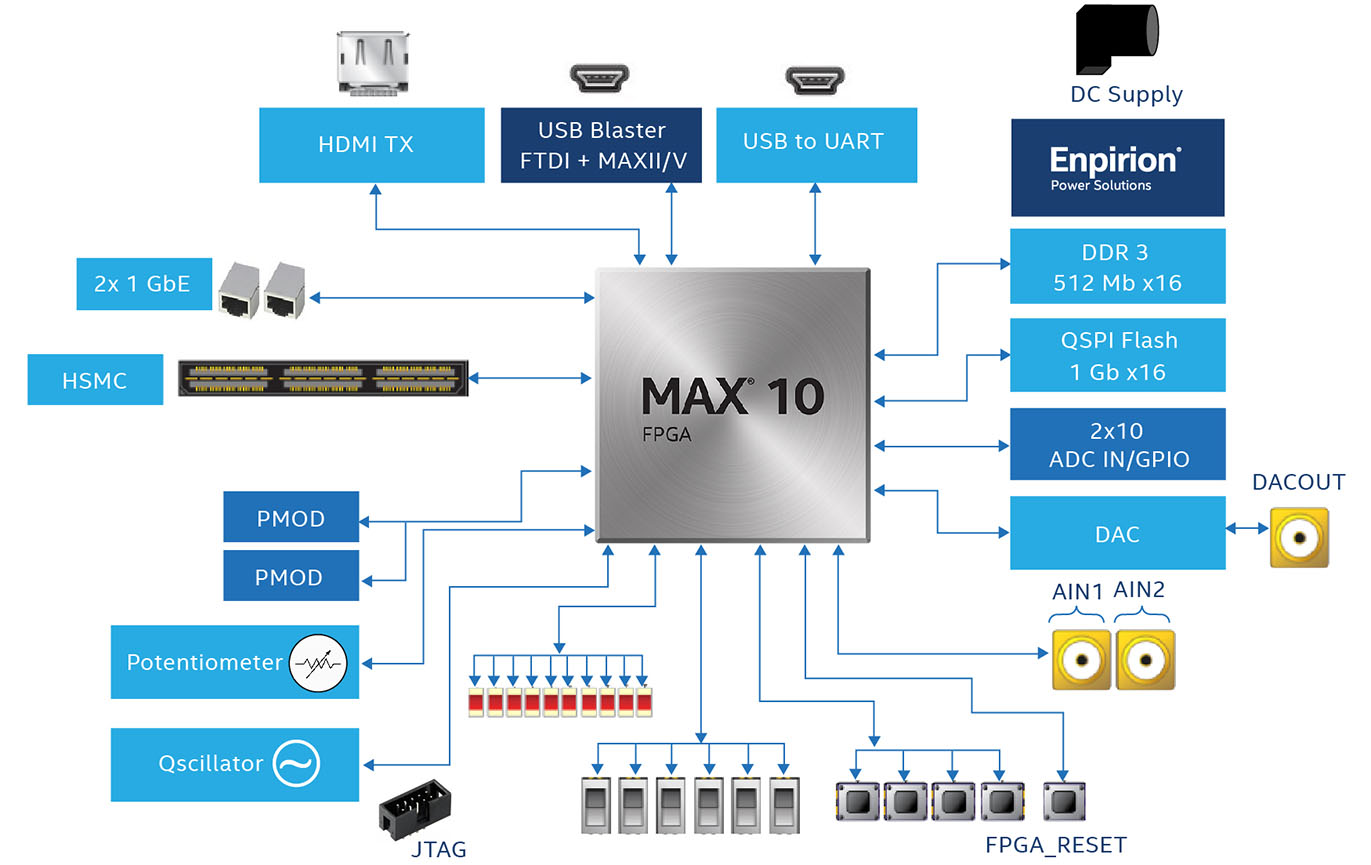
3. Block Diagram & Internal Architecture
The MAX 10 FPGA development kit block diagram below illustrates the key subsystems surrounding the 10M16 device, including the JTAG interface, power management, clock generation, memory, and I/O expansion headers. The on-chip architecture integrates logic elements, M9K embedded memory blocks, DSP multiplier blocks, PLLs, a dual ADC, user flash memory, and the configuration flash — all accessible through the Quartus Prime design environment.
4. Pinout & Package Information
The 10M16SAU169I7G uses a 169-ball UBGA (Ultra Fine-pitch Ball Grid Array) package with an 11 × 11 mm body and 0.8 mm ball pitch. The device provides 130 user I/O pins organized across four I/O banks, each with an independent VCCIO supply rail supporting voltage levels from 1.2 V to 3.3 V. Dedicated pins include JTAG (TCK, TMS, TDI, TDO), clock inputs, ADC analog inputs, and power/ground connections. The compact UBGA-169 footprint is well-suited for space-constrained designs in industrial sensor modules and IoT gateways.

For the complete pin assignment table and recommended PCB land pattern, refer to the MAX 10 FPGA Device Datasheet and the MAX 10 FPGA Package Plan available from the Altera MAX 10 device documentation hub.
5. Application Circuits & Design Examples
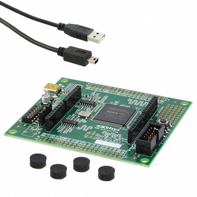
The 10M16SAU169I7G is commonly deployed in evaluation kits and production boards that combine the FPGA with external SDRAM, flash storage, Ethernet PHY, USB, and various sensor interfaces. The development kit shown below demonstrates a typical system architecture featuring DDR3 SDRAM, QSPI flash, Ethernet, HDMI output, and Arduino-compatible expansion headers — all driven by the MAX 10 FPGA with its integrated ADC sampling on-board sensors.
Typical applications for the 10M16SAU169I7G include:
- Industrial motor control — PWM generation, encoder feedback, and ADC-based current sensing in a single chip
- IoT edge gateway — Protocol bridging (SPI/I2C/UART to Ethernet), sensor data aggregation, and local preprocessing
- Power supply sequencing — Replacing CPLD-based sequencers with programmable logic and analog monitoring
- Video pre-processing — Camera interface, color-space conversion, and overlay generation for surveillance systems
- Test & measurement — High-speed data acquisition with the integrated ADC and LVDS interfaces
Video Tutorial: Intel MAX 10 FPGA Development Workflow
6. Frequently Asked Questions
What is the difference between 10M16SAU169I7G and 10M16SAU169C8G?
Both devices share the same MAX 10 die with 16,000 logic elements in a UBGA-169 package, and both feature the single-supply analog variant with integrated ADC. The key differences are temperature range and speed grade: the 10M16SAU169I7G is rated for industrial temperature (−40 °C to +100 °C) at speed grade 7, while the 10M16SAU169C8G is rated for commercial temperature (0 °C to +85 °C) at speed grade 8. The industrial variant is the appropriate choice for harsh-environment applications such as outdoor industrial controls and transportation systems.
Does the 10M16SAU169I7G require an external configuration memory?
No. The MAX 10 family includes internal flash configuration memory that stores the FPGA bitstream on-chip. This eliminates the need for an external EPCS or EPCQ serial configuration device, reduces BOM cost, and enables instant-on operation — the FPGA begins executing its design within milliseconds of power-up. The 10M16SAU169I7G supports dual configuration images for remote update with a fallback safe image.
What ADC capabilities does the 10M16SAU169I7G provide?
The 10M16SAU169I7G integrates a dual-channel 12-bit successive-approximation ADC block with up to 17 analog input channels and a maximum sample rate of 1 MSPS per ADC block. The ADC supports single-ended inputs with a voltage range of 0 V to the analog supply rail. An internal temperature sensing diode is also available. The ADC is controlled through a dedicated Quartus IP core and can be accessed from user logic via an Avalon-MM interface.
What development tools are needed to program the 10M16SAU169I7G?
The 10M16SAU169I7G is supported by Quartus Prime Lite Edition, which is free to download and use without a license file. Design entry supports Verilog HDL, VHDL, and schematic capture. Programming is done via JTAG using a USB Blaster II programmer. The Platform Designer (formerly Qsys) system integration tool and the Nios II soft-processor ecosystem are fully supported for building embedded systems on MAX 10 devices.
Can the 10M16SAU169I7G interface with DDR3 SDRAM?
Yes. The MAX 10 family supports external memory interfaces including DDR3, DDR2, and LPDDR2 SDRAM. The 10M16SAU169I7G in the U169 package provides sufficient I/O pins and dedicated DQS pins for a DDR3 x16 interface. Quartus Prime includes the EMIF (External Memory Interface) IP core to generate optimized memory controllers with calibration logic. Maximum DDR3 data rates depend on speed grade, with the device supporting up to 300 MHz (DDR3-600).
What are the power supply requirements for the 10M16SAU169I7G?
The 10M16SAU169I7G is a single-supply variant (denoted by the 'S' in the part number), requiring a 3.0 V or 3.3 V VCC supply that feeds the internal voltage regulator for the 1.2 V core. The VCCIO pins accept 1.2 V, 1.5 V, 1.8 V, 2.5 V, or 3.3 V depending on the I/O standard selected per bank. The VCCA analog supply for the ADC is 2.5 V. Altera recommends using the MAX 10 Power Management User Guide and the Early Power Estimator spreadsheet to size power regulators.
Looking for more Altera FPGA options? Browse our technical guides: 10M16SAU169C8G (Commercial Grade) · 10M08SAE144C8G (8K LE, E144) · 10M04SCE144C8G (4K LE)


