
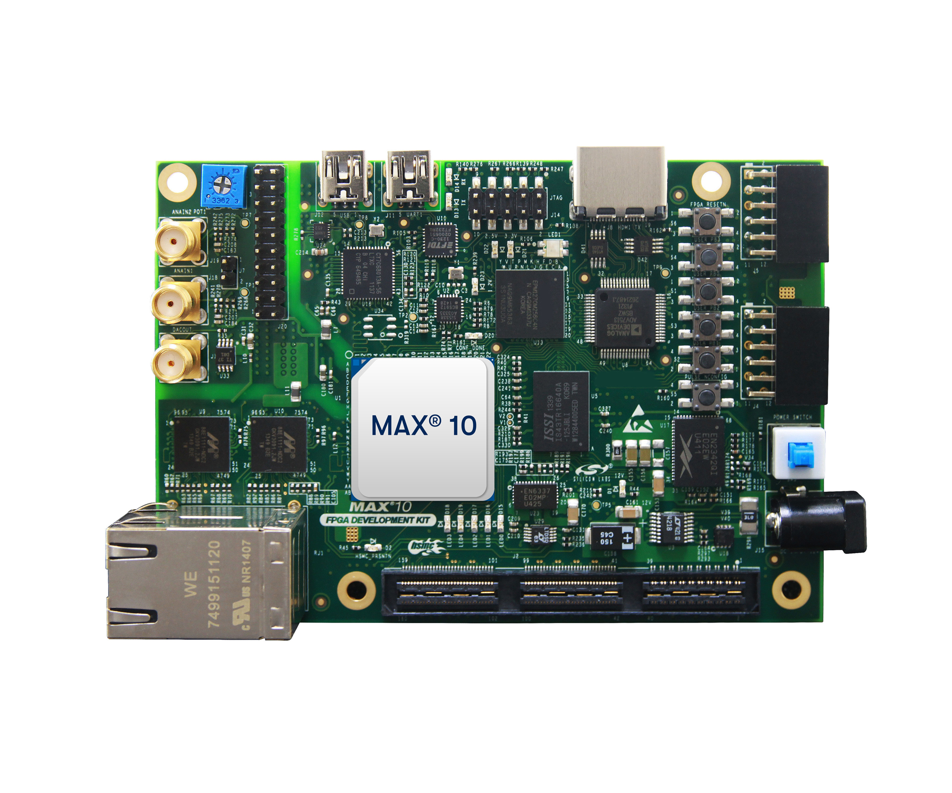
10M16SAU169I7G Datasheet, Specifications & Application Guide – Altera MAX 10 FPGA
The 10M16SAU169I7G is a non-volatile FPGA from the Altera (Intel) MAX 10 family, fabricated on a 55 nm flash process. With 16,000 logic elements, an integrated dual 12-bit ADC, instant-on configuration, and a compact 169-ball UBGA package rated for industrial temperatures (−40 °C to +100 °C), it is an ideal single-chip solution for sensor hubs, motor drives, IoT edge gateways, and mixed-signal embedded systems.
Overview & Part Number Decoding
The MAX 10 FPGA family from Altera (now part of Intel) combines non-volatile flash-based configuration with advanced FPGA fabric in a single chip. The 10M16SAU169I7G eliminates the need for an external configuration device, enabling instant-on operation within milliseconds of power-up. This makes it particularly attractive for industrial control, automotive-adjacent, and safety-critical applications where boot latency is unacceptable.
Part number breakdown:
- 10M16 – MAX 10 family, 16,000 logic elements
- S – Single power-supply
- A – Analog block enabled (integrated ADC)
- U169 – 169-ball Ultra-thin Ball Grid Array (UBGA) package
- I – Industrial temperature range (−40 °C to +100 °C)
- 7 – Speed grade 7
- G – Lead-free (RoHS compliant), green packaging
Key Specifications & Parameters
| Parameter | Value |
|---|---|
| Family | MAX 10 (Altera / Intel) |
| Logic Elements (LEs) | 16,000 |
| Embedded RAM (M9K) | 549 Kb |
| User Flash Memory (UFM) | 2,304 Kb |
| DSP Blocks (18×18 Multipliers) | 45 |
| ADC | Dual 12-bit, up to 1 MSPS |
| Maximum I/O Pins | 130 |
| PLL | 1 |
| Core Voltage | 1.2 V |
| I/O Voltage | 3.0 V / 3.3 V |
| Process Technology | 55 nm Flash |
| Package | 169-ball UBGA (11 × 11 mm) |
| Temperature Range | −40 °C to +100 °C (Industrial) |
| Speed Grade | 7 |
| Configuration | Internal flash, instant-on, dual boot image |
| RoHS Compliant | Yes |
Block Diagram & Architecture
The MAX 10 architecture integrates programmable logic, embedded memory, DSP blocks, a dual 12-bit ADC, user flash memory, and configuration flash into a single monolithic device.
Key architectural highlights include dual configuration flash images for safe remote firmware updates, a hardened ADC block that interfaces directly with the FPGA fabric through an Avalon-MM bus, and M9K memory blocks configurable as single- or dual-port RAM, ROM, or FIFO buffers.
Pinout & Package Information
The 10M16SAU169I7G is housed in a 169-ball UBGA package measuring 11 × 11 mm with a 0.8 mm ball pitch. This compact footprint makes it suitable for space-constrained PCB designs while still providing 130 user-configurable I/O pins.

The I/O pins support LVCMOS, LVTTL, SSTL, and LVDS standards. Each I/O bank has independent VCCIO supply for flexible multi-voltage interfacing.
Application Circuit & Design Guide
The 10M16SAU169I7G is commonly deployed as the central processing hub in industrial IoT, motor control, and mixed-signal data acquisition systems.
Design Recommendations
- Power Supply: Use a single 3.3 V rail with an integrated LDO or DC-DC converter for the 1.2 V core. Decouple each VCC and VCCIO pin with 100 nF + 4.7 μF capacitors.
- Configuration: Leverage the dual configuration flash for A/B boot images, enabling safe over-the-air firmware updates.
- ADC Design: Route analog input traces away from high-speed digital signals. Use a dedicated analog ground plane.
- JTAG Programming: Connect TDI, TDO, TMS, TCK with 10 kΩ pull-up/pull-down resistors as specified in the datasheet.
Video Tutorial
Watch this tutorial to get started with Intel MAX 10 FPGA development:
Frequently Asked Questions (FAQ)
1. What is the 10M16SAU169I7G?
The 10M16SAU169I7G is a non-volatile FPGA from the Altera (Intel) MAX 10 family featuring 16,000 logic elements, a dual 12-bit ADC, 549 Kb embedded RAM, 2,304 Kb user flash memory, and 45 DSP blocks in a 169-ball UBGA industrial-grade package.
2. What is the operating temperature range?
It is rated for −40 °C to +100 °C (industrial), suitable for factory automation, outdoor IoT, and transportation systems.
3. Does it require an external configuration memory?
No. The MAX 10 integrates on-chip configuration flash memory for instant-on operation. It also supports dual configuration images for safe remote updates.
4. What development tools are needed?
Quartus Prime Lite Edition (free) for synthesis and programming, plus ModelSim for simulation. Hardware programming uses a USB-Blaster cable.
5. What are common applications?
Industrial motor drives, sensor fusion hubs, IoT edge gateways, video surveillance pre-processing, medical instrumentation, and mixed-signal data acquisition systems.
6. How does the integrated ADC work?
The MAX 10 features a hardened dual 12-bit ADC (up to 1 MSPS per channel) connected via Avalon-MM bus, supporting up to 18 analog input channels and on-chip temperature sensing.


