
10M16SAU169I7G Datasheet, Specifications & Application Guide – Altera MAX 10 FPGA
1. Overview of the 10M16SAU169I7G
The 10M16SAU169I7G is a non-volatile FPGA from the Altera (Intel) MAX 10 family, fabricated on a 55 nm process node. It integrates 16,000 logic elements (LEs), embedded SRAM, user flash memory, a dual 12-bit analog-to-digital converter (ADC), and up to four PLLs—all in a compact 169-ball UBGA package. Because the configuration bitstream is stored in on-die flash, the device boots instantly without an external configuration ROM, simplifying board design and reducing BOM cost.
The part number decodes as follows: 10M16 = MAX 10 with 16K LEs, S = single power-supply mode, A = analog block (ADC enabled), U169 = 169-ball UBGA package, I = industrial temperature range (−40 °C to +100 °C), and 7 = speed grade 7 (highest performance). This combination makes the 10M16SAU169I7G an excellent choice for industrial IoT, motor control, sensor fusion, and embedded vision applications that demand high reliability across a wide temperature range.
Looking for related Altera MAX 10 devices? Browse our selection of Altera FPGA components or explore our full FPGA catalog for pin-compatible alternatives.
2. Key Specifications & Parameters
| Parameter | Value |
|---|---|
| Manufacturer | Altera (Intel) |
| Family | MAX 10 (10M16) |
| Process Node | 55 nm |
| Logic Elements (LEs) | 16,000 |
| Embedded SRAM (M9K) | 549 Kb |
| User Flash Memory (UFM) | 2,304 Kb |
| 18×18 Multipliers (DSP) | 45 |
| PLLs | 4 |
| ADC | Dual 12-bit, 1 MSPS |
| Maximum User I/O | 130 (U169 package) |
| LVDS Pairs | Up to 22 |
| I/O Standards | 3.3 V LVTTL, 1.2–3.3 V LVCMOS, SSTL, HSTL, LVDS |
| External Memory Interface | DDR2, DDR3, LPDDR2, SRAM |
| Core Voltage | 1.2 V |
| Package | 169-ball UBGA (11 × 11 mm) |
| Temperature Range | −40 °C to +100 °C (Industrial) |
| Speed Grade | 7 (Fastest) |
| Configuration | Internal flash (instant-on, no external ROM needed) |
| Bitstream Security | AES-256 encryption |
3. Block Diagram & Architecture
The MAX 10 architecture is built around an array of logic elements organized into Logic Array Blocks (LABs), surrounded by embedded memory (M9K blocks), DSP multiplier blocks, and I/O elements. The integrated dual ADC connects to an analog input multiplexer that can route up to 18 external analog channels, while the internal flash stores both the configuration image and user data. Dual-boot capability allows field upgrades with a safe fallback image.
Figure 1: Block diagram of the Intel MAX 10 FPGA architecture highlighting the logic fabric, embedded memory, DSP multipliers, PLL, ADC, and user flash memory blocks.
4. Pinout & Package Information
The 10M16SAU169I7G uses a 169-ball UBGA (Ultra-Fine-Pitch Ball Grid Array) package with a 0.8 mm ball pitch and a total body size of approximately 11 × 11 mm. The compact form factor makes it suitable for space-constrained designs. The 130 user I/O pins are organized across multiple I/O banks, each independently configurable for voltage levels from 1.2 V to 3.3 V. Dedicated clock inputs, JTAG pins, and analog input channels are allocated to specific ball locations per the official pin-out table.

Figure 2: The Altera MAX 10 FPGA in a UBGA package, representative of the 10M16SAU169I7G 169-ball configuration.
5. Typical Applications & Circuit Design
The 10M16SAU169I7G is widely deployed in industrial automation, motor drives, sensor hubs, IoT edge gateways, video surveillance pre-processing, medical instrumentation, and test & measurement equipment. Its instant-on configuration, integrated ADC, and robust industrial temperature rating make it an ideal single-chip solution where a separate MCU + FPGA combination would otherwise be required.
For rapid prototyping, the Terasic DE10-Lite and the Arrow BeMicro MAX 10 evaluation boards both feature MAX 10 FPGAs with on-board USB-Blaster programming, SDRAM, and expansion headers. The free Quartus Prime Lite Edition provides a complete design flow including synthesis, place-and-route, timing analysis, and JTAG programming.
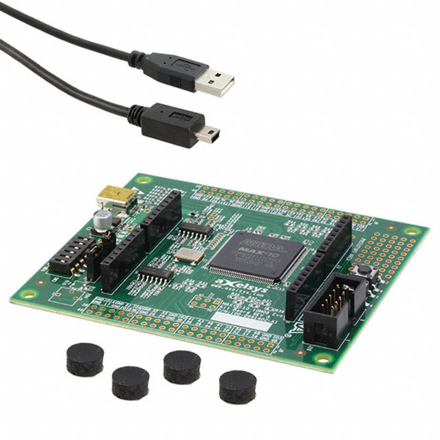
Figure 3: A MAX 10 FPGA evaluation kit—ideal for prototyping designs based on the 10M16SAU169I7G before moving to production.
Need development tools or companion ICs? Check out our Intel semiconductor catalog for power regulators, level shifters, and other support components commonly used alongside MAX 10 FPGAs.
Video Tutorial: Getting Started with Intel MAX 10 FPGA
6. Frequently Asked Questions (FAQ)
What is the 10M16SAU169I7G?
The 10M16SAU169I7G is a non-volatile FPGA from the Altera (Intel) MAX 10 family. It contains 16,000 logic elements, 549 Kb of embedded SRAM, 2,304 Kb of user flash memory, a dual 12-bit ADC, and 4 PLLs in a 169-ball UBGA package rated for the industrial temperature range (−40 °C to +100 °C) at speed grade 7.
What is the operating temperature range of the 10M16SAU169I7G?
The 10M16SAU169I7G is rated for the industrial temperature range of −40 °C to +100 °C, as indicated by the "I" suffix in the part number. This makes it suitable for harsh-environment applications such as factory automation, outdoor IoT deployments, and automotive-adjacent systems.
Does the 10M16SAU169I7G have an integrated ADC?
Yes. The "A" in the part number indicates the analog block is enabled. The device includes a dual 12-bit ADC capable of 1 MSPS with up to 18 analog input channels through an internal multiplexer, eliminating the need for an external ADC in many sensor-interface designs.
What package does the 10M16SAU169I7G use?
The device uses a 169-ball UBGA (Ultra-Fine-Pitch Ball Grid Array) package with a 0.8 mm ball pitch and approximate body dimensions of 11 × 11 mm. It provides 130 user I/O pins across multiple independently configurable I/O banks.
Does the 10M16SAU169I7G require an external configuration memory?
No. The MAX 10 family stores its configuration bitstream in on-die flash memory, enabling instant-on operation without any external configuration ROM or PROM. This simplifies board design, reduces BOM cost, and supports dual-boot capability for safe in-field firmware updates.
What software tools are needed to program the 10M16SAU169I7G?
You can use the free Quartus Prime Lite Edition from Intel/Altera, which provides a complete design flow including HDL synthesis (Verilog/VHDL), place-and-route, timing analysis, and JTAG/USB-Blaster programming. Evaluation boards like the Terasic DE10-Lite and Arrow BeMicro MAX 10 include on-board programmers for quick development.


