
The 10M16SAU169I7G is a non-volatile FPGA from the Intel (formerly Altera) MAX 10 family, built on a 55 nm process node. Featuring 16,000 logic elements, an integrated dual 12-bit ADC, and instant-on configuration from internal flash memory, this device is ideal for industrial IoT, motor control, sensor fusion, and mixed-signal embedded designs. Its single-supply operation and compact 169-ball UBGA package make it an excellent choice for space-constrained applications requiring analog integration.
Table of Contents
- Key Specifications & Parameters
- Block Diagram & Architecture
- Pinout & Package Information
- Application Circuit & Design Guide
- Development Tools & Resources
- Frequently Asked Questions (FAQ)
Key Specifications & Parameters
The following table summarizes the critical electrical and mechanical parameters of the 10M16SAU169I7G FPGA. These specifications are essential for PCB layout, power supply design, and system integration.
| Parameter | Value |
|---|---|
| Manufacturer | Intel (Altera) |
| Family | MAX 10 FPGA |
| Part Number | 10M16SAU169I7G |
| Logic Elements (LEs) | 16,000 |
| Embedded Memory (M9K) | 549 Kbit |
| User Flash Memory (UFM) | 2,304 Kbit |
| DSP Multipliers (18×18) | 45 |
| PLLs | 4 |
| User I/O Pins | 130 |
| ADC | Dual 12-bit, 1 MSPS |
| Core Voltage | 1.2 V |
| I/O Voltage | 3.3 V (single supply) |
| Package | 169-ball UBGA (11 × 11 mm) |
| Temperature Range | −40 °C to +100 °C (Industrial) |
| Speed Grade | 7 |
| Process Technology | 55 nm |
| Configuration | Internal flash (instant-on) |
| Memory Interface Support | DDR2, DDR3, LPDDR2 |
| Supply Mode | Single supply (S variant) |
Block Diagram & Architecture
The MAX 10 FPGA architecture integrates logic elements, embedded memory blocks, DSP multipliers, PLLs, and a dual 12-bit ADC into a single non-volatile device. The internal flash configuration memory enables instant-on operation without an external configuration device, simplifying the BOM and reducing board space.
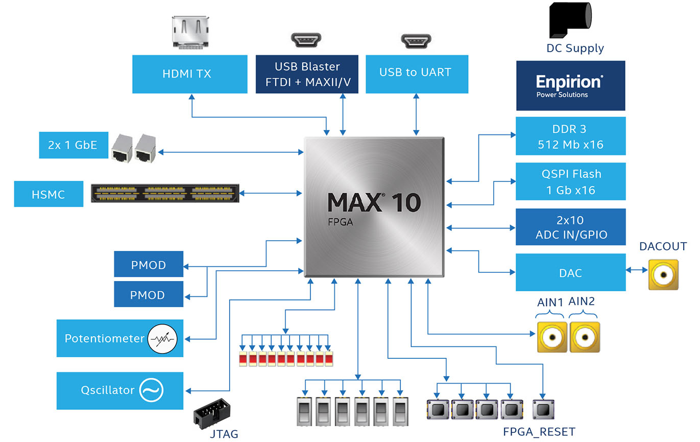
The architecture features adaptive logic modules (ALMs) organized into logic array blocks (LABs), with M9K embedded memory blocks providing up to 549 Kbit of on-chip RAM. The 45 embedded 18×18 multipliers enable efficient DSP operations for signal processing applications.
Pinout & Package Information
The 10M16SAU169I7G uses a 169-ball Ultra Fine-pitch Ball Grid Array (UBGA) package with an 11 × 11 mm body size and 0.8 mm ball pitch. This compact form factor provides 130 user I/O pins across multiple I/O banks supporting LVDS, LVCMOS, and SSTL signaling standards.
The UBGA-169 package supports DDR2/DDR3 memory interfaces and provides dedicated configuration pins, JTAG programming pins, and analog input channels for the integrated ADC. The compact footprint makes it suitable for designs where board real estate is at a premium.
Application Circuit & Design Guide
The 10M16SAU169I7G is widely deployed in industrial automation, motor drive controllers, IoT edge gateways, medical instrumentation, and video surveillance preprocessing systems. Its integrated ADC eliminates the need for external analog-to-digital converters, reducing component count and simplifying PCB routing.
For a typical application circuit, the single-supply design requires only a 3.3 V input rail with internal regulators generating the 1.2 V core supply. Decoupling capacitors (100 nF ceramic per power pin plus bulk 10 µF) should be placed close to the FPGA. The JTAG interface (TCK, TMS, TDI, TDO) connects to an Intel USB Blaster for programming and debugging via Quartus Prime Lite.
Development Tools & Resources
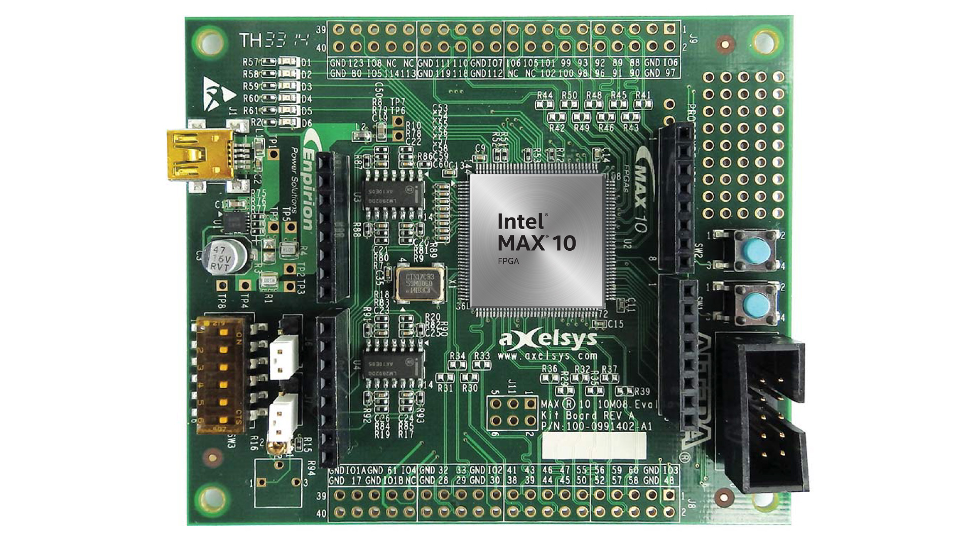
Intel provides comprehensive development support for the MAX 10 family through the free Quartus Prime Lite Edition, which includes synthesis, place-and-route, timing analysis, and JTAG programming tools. Popular development boards include the Terasic DE10-Lite and the Intel MAX 10 FPGA Evaluation Kit.
Video Tutorial: Getting Started with MAX 10 FPGA
The MAX 10 device family is supported by a rich ecosystem including Nios II soft processor, Platform Designer (formerly Qsys) for system integration, and ModelSim for simulation. The Intel FPGA University Program provides additional teaching materials and design examples.
Frequently Asked Questions (FAQ)
What is the 10M16SAU169I7G?
The 10M16SAU169I7G is a non-volatile FPGA from Intel's MAX 10 family with 16,000 logic elements, a dual 12-bit ADC, 549 Kbit embedded memory, and 2,304 Kbit user flash memory in a 169-ball UBGA package. It operates across the industrial temperature range of −40 °C to +100 °C.
What does the part number 10M16SAU169I7G decode to?
10M = MAX 10 family, 16 = 16,000 LEs, S = single supply, A = analog (ADC enabled), U169 = 169-ball UBGA package, I = industrial temperature, 7 = speed grade 7, G = lead-free (RoHS compliant).
Does the 10M16SAU169I7G require an external configuration device?
No. The MAX 10 FPGA stores its configuration in internal flash memory, enabling instant-on operation at power-up without any external EEPROM or flash configuration device. This reduces BOM cost and simplifies board design.
What development tools are needed for the 10M16SAU169I7G?
You need Intel Quartus Prime Lite Edition (free download) for design entry, synthesis, and programming. An Intel USB Blaster or USB Blaster II cable is required for JTAG programming. Popular evaluation boards include the Terasic DE10-Lite and the Intel MAX 10 FPGA Development Kit.
What are the power supply requirements for the 10M16SAU169I7G?
The 10M16SAU169I7G is a single-supply variant requiring only a 3.3 V input supply. Internal voltage regulators generate the 1.2 V core supply from the 3.3 V input, simplifying power design and reducing external component count.
What applications is the 10M16SAU169I7G best suited for?
This FPGA excels in industrial control systems, motor drives, sensor hubs, IoT edge gateways, video surveillance preprocessing, medical instrumentation, and any application requiring mixed-signal capabilities with the integrated 12-bit ADC and instant-on non-volatile configuration.
Looking for more FPGA components? Browse our full range of FPGA and CPLD devices or explore Intel FPGA solutions for your next design project.


