
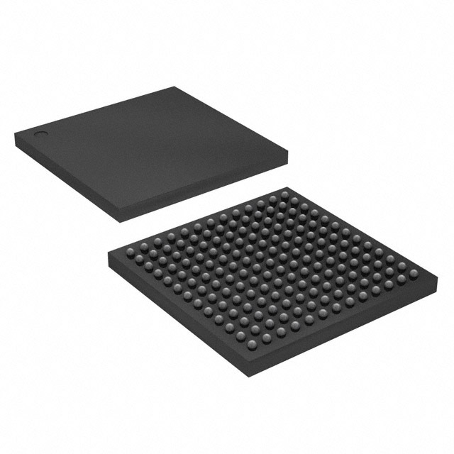
1. 10M16SAU169I7G Overview
The 10M16SAU169I7G is a non-volatile FPGA from the Altera (Intel) MAX 10 family, built on a mature 55 nm TSMC process. As a single-chip, instant-on programmable logic device, it eliminates the need for an external configuration flash, making it an ideal drop-in replacement for complex CPLDs and low-density FPGAs in space-constrained industrial designs.
The part number decodes as follows: 10M16 = MAX 10 family with 16,000 logic elements, S = single-supply operation, A = analog block enabled (dual ADC), U169 = 169-ball UBGA package (11 × 11 mm), I = industrial temperature range (−40 °C to +100 °C), and 7 = speed grade 7.
With integrated dual 12-bit ADCs, user flash memory, and a compact UBGA-169 footprint, the 10M16SAU169I7G is widely deployed in motor control, sensor fusion hubs, IoT edge gateways, industrial automation, and medical instrumentation. If you need the commercial temperature variant, consider the 10M16SAU169C8G.
2. Key Specifications & Parameters
| Parameter | Value |
|---|---|
| Manufacturer | Altera (Intel) |
| Family | MAX 10 (10M) |
| Part Number | 10M16SAU169I7G |
| Logic Elements (LEs) | 16,000 |
| Logic Array Blocks (LABs) | 1,000 |
| Embedded Memory (M9K) | 549 Kb (60 M9K blocks) |
| User Flash Memory (UFM) | 2,304 Kb |
| 18 × 18 Multipliers | 45 |
| Phase-Locked Loops (PLLs) | 4 |
| Global Clock Networks | 20 |
| Analog-to-Digital Converter | Dual 12-bit, 1 MSPS ADC |
| Maximum User I/O (U169) | 130 |
| LVDS Pairs (U169) | Up to 22 |
| Package | 169-ball UBGA (11 × 11 mm, 0.8 mm pitch) |
| Core Voltage | 1.2 V |
| I/O Voltage | 1.2 V / 1.5 V / 1.8 V / 2.5 V / 3.0 V / 3.3 V |
| Operating Temperature | −40 °C to +100 °C (Industrial) |
| Speed Grade | 7 (slowest) |
| Process Technology | 55 nm |
| Configuration | Internal flash (instant-on, < 10 ms) |
| External Memory Interface | DDR3, DDR3L, DDR2, LPDDR2 |
| RoHS Compliant | Yes |
3. Block Diagram & Architecture
The MAX 10 architecture integrates programmable logic, embedded memory, DSP blocks, PLLs, ADC blocks, and user flash memory in a single die. The block diagram below illustrates the high-level architecture of the MAX 10 FPGA family, showing the interconnection between logic array blocks (LABs), M9K embedded memory, DSP multiplier blocks, clock networks, I/O elements, and the on-chip analog-to-digital converters.

Key architectural highlights include instant-on configuration from internal flash memory (boot time under 10 ms), dual-image support for safe remote firmware updates, and integrated analog-to-digital conversion that eliminates external ADC components for mixed-signal applications.
4. Pinout & Package Information
The 10M16SAU169I7G is housed in a 169-ball UBGA package with an 11 × 11 mm body size and 0.8 mm ball pitch. Of the 169 balls, 130 are available as user I/O pins organized across multiple I/O banks supporting a wide range of single-ended (LVTTL, LVCMOS) and differential (LVDS, SSTL, HSTL) I/O standards.
For pin assignments and board-level design, refer to the official MAX 10 FPGA Pin-Out Files available from the Altera MAX 10 product page. When using the integrated ADC, dedicated analog input pins must be reserved and cannot be used as general-purpose I/O. The JTAG configuration pins (TCK, TDI, TDO, TMS) are also fixed-function.
5. Application Circuits & Development
The 10M16SAU169I7G is well-suited for a wide range of embedded applications. Its single-chip integration of logic, memory, DSP, and ADC makes it an excellent platform for:
- Industrial Motor Control – PWM generation, encoder interfaces, and PID control loops
- Sensor Fusion Hubs – On-chip ADC for temperature, pressure, and current sensing with digital processing
- IoT Edge Gateways – Protocol bridging (SPI, I²C, UART) with local data preprocessing
- Video Preprocessing – Frame buffering, color-space conversion, and scaling for surveillance cameras
- Medical Instrumentation – Signal acquisition and filtering for patient monitoring devices
Development is supported by the free Quartus Prime Lite Edition, which includes synthesis, place-and-route, timing analysis, and JTAG/AS programming. Popular development boards include the Terasic DE10-Lite and the Intel MAX 10 FPGA Development Kit, both of which provide USB-Blaster programming, SDRAM, and expansion headers for prototyping. For purchasing the 10M16SAU169I7G or compatible boards, visit the wwdparts.com product page.
Video: Getting Started with MAX 10 FPGA
6. Frequently Asked Questions
What is the 10M16SAU169I7G?
The 10M16SAU169I7G is a non-volatile FPGA from the Intel (Altera) MAX 10 family. It features 16,000 logic elements, 549 Kb of embedded RAM, 2,304 Kb of user flash memory, 45 DSP multipliers, dual 12-bit ADCs, and 130 user I/O pins in a compact 169-ball UBGA package with industrial temperature range (−40 °C to +100 °C).
What is the difference between 10M16SAU169I7G and 10M16SAU169C8G?
Both share the same 16K LE logic fabric and UBGA-169 package. The key differences are: the "I7G" variant operates over the industrial temperature range (−40 °C to +100 °C) at speed grade 7, while the "C8G" variant covers the commercial range (0 °C to +85 °C) at speed grade 8. Choose the I7G for harsh-environment or extended-temperature applications.
Does the 10M16SAU169I7G require an external configuration memory?
No. The MAX 10 family integrates on-chip configuration flash memory, enabling instant-on operation (boot time under 10 ms) without any external configuration PROM or SPI flash. This reduces BOM cost, board area, and system complexity compared to SRAM-based FPGAs.
What development tools are needed for the 10M16SAU169I7G?
Intel's free Quartus Prime Lite Edition fully supports all MAX 10 devices, including the 10M16SAU169I7G. It provides HDL synthesis (Verilog/VHDL), place-and-route, timing analysis, the Platform Designer (Qsys) system integration tool, and JTAG/AS programming support. ModelSim-Intel Starter Edition is included for simulation.
What are the power supply requirements for the 10M16SAU169I7G?
The device requires a 1.2 V core supply (VCC) and supports I/O bank voltages of 1.2 V, 1.5 V, 1.8 V, 2.5 V, 3.0 V, and 3.3 V. The single-supply variant (S in the part number) uses internal regulators to simplify the power tree—only VCCIO and VCC supplies are needed for basic operation.
Can the 10M16SAU169I7G interface with DDR3 memory?
Yes. The MAX 10 family supports DDR3, DDR3L, DDR2, and LPDDR2 external memory interfaces. The 10M16 in the U169 package can drive DDR3 at up to 300 MHz (600 Mbps) using the hard memory controller IP available in Quartus Prime. Note that the available data width depends on the number of I/O pins in the specific package variant.


