
10M16SAU169I7G Datasheet, Specifications & Application Guide – Altera MAX 10 FPGA
The 10M16SAU169I7G is a non-volatile FPGA from the Altera (Intel) MAX 10 family, offering 16,000 logic elements, an integrated dual 12-bit ADC, and instant-on configuration from internal flash memory. Built on a 55 nm process, this industrial-grade device in a compact 169-ball UBGA package is ideal for sensor hubs, motor control, IoT edge processing, and mixed-signal embedded systems. This comprehensive guide covers its full datasheet specifications, pinout, block diagram, typical application circuits, and design best practices.
Table of Contents
- 1. 10M16SAU169I7G Overview
- 2. Key Specifications & Parameters
- 3. Block Diagram & Architecture
- 4. Pinout & Package Information
- 5. Typical Application Circuit & Design Guide
- 6. FAQ – Frequently Asked Questions
1. 10M16SAU169I7G Overview
The 10M16SAU169I7G belongs to the Intel (formerly Altera) MAX 10 FPGA family, which uniquely combines non-volatile configuration storage, a programmable logic fabric, and an analog-to-digital converter on a single chip. The "S" in the part number indicates single-supply operation (powered from a single 3.3 V rail), while the "A" denotes the presence of the on-chip ADC block. The U169 package provides 130 user I/O pins in an ultra-compact 11 × 11 mm BGA footprint, making it well-suited for space-constrained industrial and IoT applications.
Unlike traditional FPGAs that require external configuration flash, the MAX 10 stores up to two configuration images in its internal flash, enabling instant-on operation in under 10 ms and supporting secure dual-image boot with automatic fallback. The device is supported by the free Quartus Prime Lite Edition toolchain.
2. Key Specifications & Parameters
| Parameter | Value |
|---|---|
| Part Number | 10M16SAU169I7G |
| Family | Intel (Altera) MAX 10 |
| Process Node | 55 nm |
| Logic Elements (LEs) | 16,000 |
| Logic Array Blocks (LABs) | 1,000 |
| Embedded RAM (M9K) | 549 Kb (61 M9K blocks) |
| User Flash Memory (UFM) | 2,304 Kb |
| 18 × 18 Multipliers | 45 |
| PLLs | 4 |
| ADC | Dual 12-bit SAR, up to 1 MSPS, 18 analog input channels |
| Maximum User I/O (U169) | 130 |
| Maximum LVDS Pairs | 22 |
| Package | 169-ball UBGA (11 × 11 mm, 0.8 mm pitch) |
| Supply Voltage | 3.3 V single supply |
| I/O Standards | 3.3 V / 2.5 V / 1.8 V / 1.5 V LVCMOS/LVTTL, SSTL, HSTL, LVDS |
| External Memory Interface | DDR3, DDR3L, DDR2, LPDDR2 |
| Configuration | Internal flash, dual boot image, instant-on (< 10 ms) |
| Operating Temperature | −40 °C to +100 °C (Industrial) |
| Speed Grade | 7 (slowest) |
| ESD Rating | HBM Class 2 |
| Moisture Sensitivity | MSL-3 |
| RoHS | Compliant (lead-free) |
3. Block Diagram & Architecture
The MAX 10 architecture integrates a logic fabric of adaptive logic modules (ALMs) organized into LABs, embedded M9K memory blocks, DSP blocks with 18 × 18 multipliers, and four PLLs for flexible clock management. The on-chip dual 12-bit ADC with up to 18 analog input channels enables direct sensor interfacing without external ADC ICs. Internal flash memory stores configuration bitstreams and user data, eliminating the need for external configuration devices.
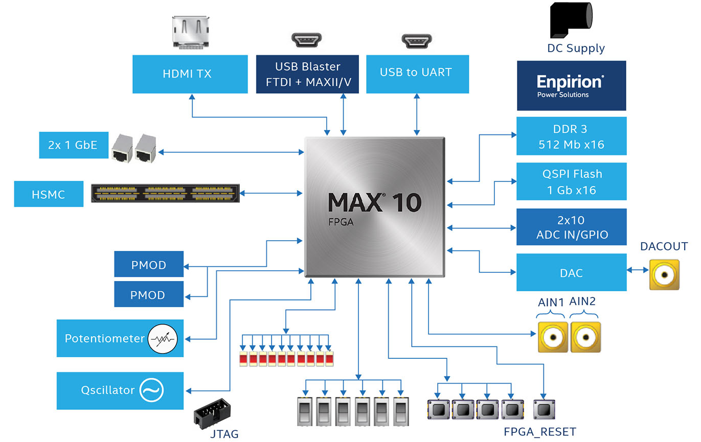
Figure 1: MAX 10 FPGA functional block diagram illustrating the internal architecture and peripheral connectivity.
4. Pinout & Package Information
The 10M16SAU169I7G is housed in a 169-ball UBGA package with a 13 × 13 ball array at 0.8 mm pitch. The package measures 11 × 11 × 1.0 mm. Out of 169 balls, 130 are available as user I/O, organized across multiple I/O banks supporting a wide range of voltage standards from 1.2 V to 3.3 V. Dedicated pins include JTAG (TCK, TMS, TDI, TDO), configuration pins, analog input channels for the ADC, and power/ground connections. Designers should refer to the official Intel MAX 10 Pin-Out Files for exact ball assignments.

Figure 2: 10M16SAU169I7G in 169-ball UBGA package – component photo.
5. Typical Application Circuit & Design Guide
A typical 10M16SAU169I7G design requires a single 3.3 V power supply, with on-chip regulators generating the 1.2 V core voltage. Decoupling capacitors (100 nF ceramic + 10 µF bulk) should be placed close to each VCC and VCCIO pin. The JTAG interface (directly or via USB-Blaster) is used for programming and debugging. For ADC applications, analog inputs should be routed with proper guard traces and filtered with RC low-pass networks to minimize noise.
The MAX 10 FPGA Development Kit and the popular Terasic DE10-Lite evaluation board provide complete reference designs with USB programming, SDRAM, VGA output, accelerometer, and Arduino-compatible headers — excellent starting points for prototyping with the 10M16SAU169I7G.
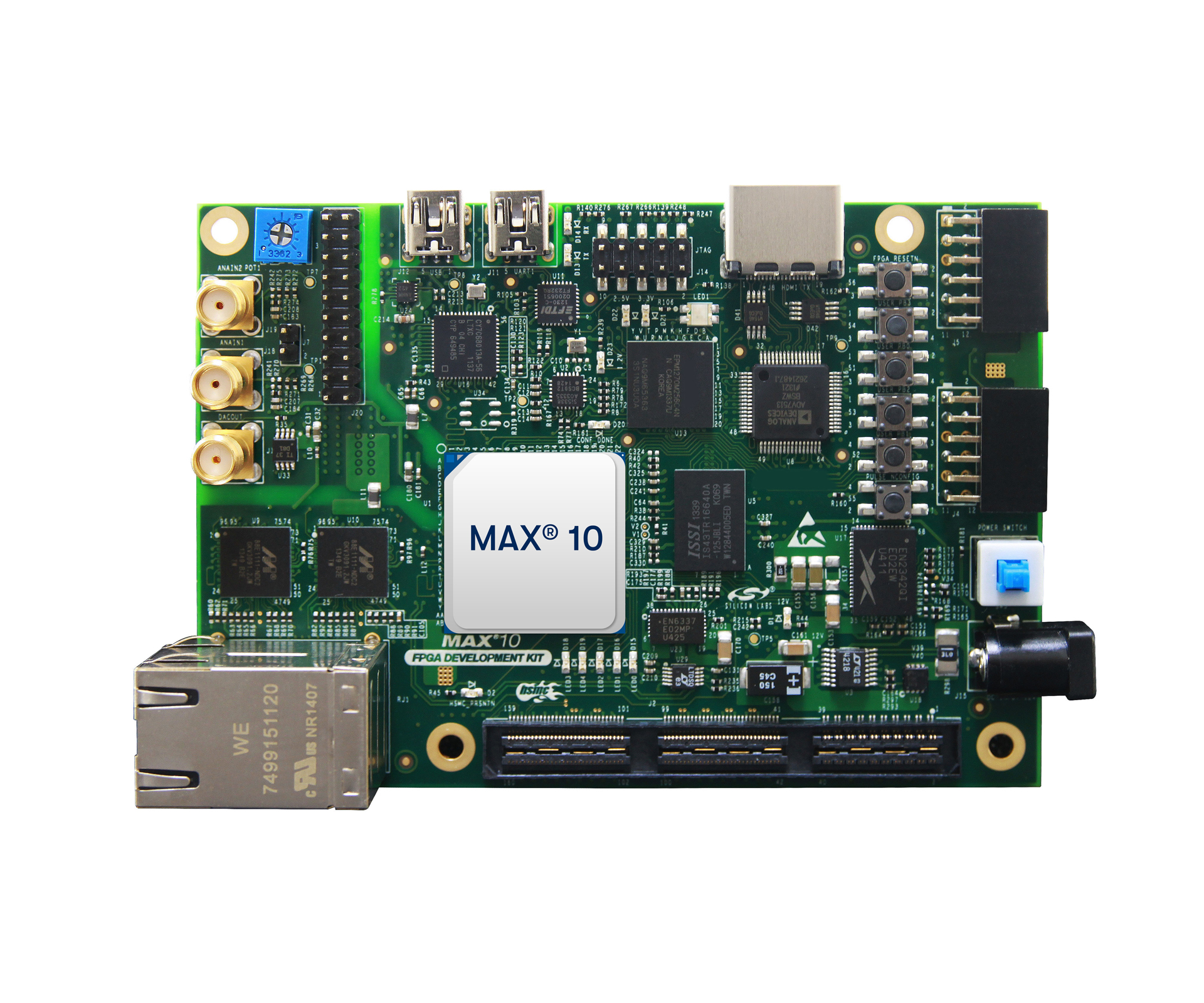
Figure 3: MAX 10 FPGA Development Kit – reference application board for prototyping and evaluation.
Design Tips
- Power: Use a low-noise 3.3 V LDO or DC-DC converter. Place bulk and bypass capacitors per Intel's power guidelines.
- Configuration: Enable dual-boot for fail-safe remote updates. Use the internal flash for both FPGA configuration and user data storage.
- ADC Layout: Isolate analog input traces from digital signals. Use a dedicated analog ground plane connected to the main ground at a single point.
- Clocking: Use the on-chip PLLs to generate required clock frequencies from a single external oscillator (e.g., 50 MHz).
- Thermal: The U169 package has an exposed thermal pad — ensure proper solder connection to the PCB ground plane for heat dissipation.
Video Tutorial: Getting Started with MAX 10 FPGA
6. FAQ – Frequently Asked Questions
Q1: What is the difference between 10M16SAU169I7G and 10M16SAU169C8G?
The main differences are temperature range and speed grade. The "I7G" variant operates over the industrial range (−40 °C to +100 °C) at speed grade 7, while the "C8G" is rated for the commercial range (0 °C to +85 °C) at speed grade 8. Both share the same logic resources, package, and ADC capability. Choose the I7G for harsh-environment or extended-temperature applications.
Q2: Does the 10M16SAU169I7G require an external configuration flash?
No. The MAX 10 family features internal configuration flash memory that stores up to two FPGA configuration images. This enables instant-on operation (configuration completes in under 10 ms at power-up) and eliminates the BOM cost and board space of an external flash device.
Q3: How many analog input channels does the 10M16SAU169I7G ADC support?
The on-chip ADC block provides a dual 12-bit successive-approximation register (SAR) converter with up to 18 analog input channels (active channels depend on the pin-out and I/O bank configuration). It supports sample rates up to 1 MSPS and includes an internal temperature sensor and voltage monitor.
Q4: What software tools are needed to program the 10M16SAU169I7G?
Intel's Quartus Prime Lite Edition (free, no license required) fully supports all MAX 10 devices, including synthesis, place-and-route, timing analysis, and JTAG/USB-Blaster programming. ModelSim Intel FPGA Starter Edition is available for simulation. The Nios II soft processor can also be instantiated for embedded software development.
Q5: Can the 10M16SAU169I7G interface with DDR3 memory?
Yes. The MAX 10 FPGA supports DDR3, DDR3L, DDR2, and LPDDR2 external memory interfaces through dedicated hard memory controller IP in supported packages. However, DDR3 support availability depends on the specific package and I/O bank configuration — verify compatibility for the U169 package using the Intel Memory Interface Pin Planner.
Q6: What is the maximum operating frequency of the 10M16SAU169I7G?
The speed grade 7 (slowest) variant achieves typical Fmax values of 200–300 MHz for simple register-to-register paths, depending on design complexity and resource utilization. For timing-critical designs requiring higher performance, consider the speed grade 6 variant (10M16SAU169I7G would be 10M16SAU169I6G). Always run timing analysis in Quartus to verify your specific design meets frequency targets.
Looking for more FPGA and semiconductor components? Browse our catalog:


