
10M16SAU169I7G Datasheet, Specifications & Application Guide – Altera MAX 10 FPGA
Overview of the 10M16SAU169I7G
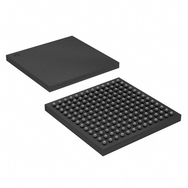
The 10M16SAU169I7G is a non-volatile FPGA from the Altera (now Intel) MAX 10 family, fabricated on a 55 nm process node. It integrates 16,000 logic elements, a dual 12-bit analog-to-digital converter (ADC), 549 Kb of embedded SRAM, and 2,304 Kb of user flash memory into a compact 169-ball UBGA package. The device operates from a single 3.3 V supply and supports an industrial temperature range of –40 °C to +100 °C, making it well-suited for harsh-environment embedded applications.
Unlike SRAM-based FPGAs that require external configuration memory, the MAX 10 stores its bitstream in on-chip flash, enabling instant-on operation within milliseconds of power-up. The integrated ADC eliminates the need for an external converter in mixed-signal designs, reducing board area and BOM cost. These features position the 10M16SAU169I7G as a versatile single-chip solution for sensor interfacing, industrial control, and IoT edge processing.
Key Specifications & Electrical Parameters
| Parameter | Value |
|---|---|
| Part Number | 10M16SAU169I7G |
| Family | Intel (Altera) MAX 10 |
| Logic Elements (LEs) | 16,000 |
| Embedded SRAM | 549 Kb |
| User Flash Memory (UFM) | 2,304 Kb |
| 18 × 18 Multipliers | 45 |
| PLLs | 2 |
| ADC | Dual 12-bit, 1 MSPS |
| Maximum User I/O Pins | 130 |
| Core Voltage | 1.2 V (internal) |
| I/O Voltage | 3.0 V / 3.3 V |
| Package | UBGA-169 (11 × 11 mm) |
| Operating Temperature | –40 °C to +100 °C (Industrial) |
| Speed Grade | 7 |
| Process Node | 55 nm |
| Configuration | Internal flash (instant-on) |
| I/O Standards Supported | LVTTL, LVCMOS, SSTL, LVDS |
Block Diagram & Internal Architecture
The MAX 10 architecture organizes logic elements into Logic Array Blocks (LABs), each containing 16 adaptive logic modules (ALMs). Embedded memory blocks are distributed throughout the fabric as M9K blocks providing 9 Kb each. The dual ADC block connects directly to a dedicated analog input multiplexer, enabling up to 18 analog channels to be sampled without external circuitry.

The on-chip flash controller manages both configuration flash memory (CFM) for FPGA bitstream storage and user flash memory (UFM) for application data. Two independent PLLs provide flexible clock synthesis with up to five output clocks each, supporting frequency multiplication, division, and phase shifting. The global clock network distributes low-skew clocks throughout the device via dedicated routing resources.
Pinout, Package & Thermal Information
The 10M16SAU169I7G is housed in a 169-ball UBGA package measuring 11 × 11 mm with a 0.8 mm ball pitch. This ultra-compact form factor is ideal for space-constrained designs such as sensor modules and compact industrial controllers. The package provides 130 user I/O pins organized across four I/O banks, each independently configurable for different voltage standards.
Thermal characteristics include a junction-to-ambient thermal resistance (θJA) of approximately 30 °C/W. For designs operating near the maximum junction temperature of 100 °C, adequate PCB copper area and airflow should be provided. The UBGA package supports standard BGA assembly processes with lead-free (RoHS-compliant) solder balls.
Typical Applications & Design Examples
The 10M16SAU169I7G serves a wide range of embedded applications that benefit from its combination of programmable logic, integrated ADC, and instant-on configuration:
- Industrial Automation: Motor drive control, PLC I/O expansion, real-time sensor fusion
- IoT Edge Processing: Sensor hub aggregation, protocol bridging (SPI/I²C to Ethernet), low-latency data preprocessing
- Medical Instruments: Patient monitoring front-ends, ultrasound signal conditioning, portable diagnostic devices
- Video & Display: LVDS panel timing controllers, video format conversion, LED display drivers
- Communications: PCIe-to-custom-bus bridging, protocol offload engines, base station auxiliary processing

Altera provides the MAX 10 FPGA Evaluation Kit and the popular Terasic DE10-Lite board for rapid prototyping. Both boards include USB-Blaster JTAG programming, on-board SDRAM, and Arduino-compatible expansion headers. The free Quartus Prime Lite Edition toolchain supports synthesis, place-and-route, timing analysis, and in-system debugging via SignalTap II for all MAX 10 devices.
Video Tutorial: Getting Started with MAX 10 FPGA
Frequently Asked Questions
What is the difference between the 10M16SAU169I7G and 10M16SAU169C8G?
Both devices share the same 16,000-LE MAX 10 die in a UBGA-169 package. The key differences are temperature range and speed grade: the I7G variant is rated for the industrial range (–40 °C to +100 °C) at speed grade 7, while the C8G variant covers the commercial range (0 °C to +85 °C) at speed grade 8. Choose the I7G for applications exposed to wide temperature swings or harsh operating environments.
Does the 10M16SAU169I7G require external configuration memory?
No. The MAX 10 family stores its configuration bitstream in on-chip flash memory, eliminating the need for an external EEPROM or flash chip. This enables instant-on operation—the FPGA is fully configured and functional within milliseconds of power-up, which is critical for safety-related and always-ready systems.
How do I use the integrated ADC on the 10M16SAU169I7G?
The dual 12-bit ADC is enabled by the "A" suffix in the part number. In Quartus Prime, instantiate the ADC IP core using the Platform Designer (Qsys) tool, which provides an Avalon-MM interface for reading conversion results. The ADC supports up to 18 analog input channels via an internal multiplexer, with a maximum sampling rate of 1 MSPS. Analog inputs are routed to dedicated pins on the UBGA-169 package.
What development tools are needed for the 10M16SAU169I7G?
You need Quartus Prime Lite Edition, which is free and supports all MAX 10 devices. It includes synthesis, fitter, timing analyzer, and the SignalTap II logic analyzer for in-system debugging. For hardware programming, a USB-Blaster or USB-Blaster II JTAG cable is required. Development boards like the Terasic DE10-Lite include an on-board USB-Blaster.
Can the 10M16SAU169I7G implement a soft processor?
Yes. The 16,000-LE fabric can accommodate the Nios II/e (economy) soft processor with room for peripherals and custom logic. For more demanding applications, the Nios II/f (fast) variant can also fit, though it consumes more logic resources. The integrated user flash memory (2,304 Kb) can store application firmware, enabling a complete single-chip embedded system.
Where can I buy the 10M16SAU169I7G and what is its availability?
The 10M16SAU169I7G is available from authorized distributors including WWDParts, Mouser, Digi-Key, and Arrow. As a current-production MAX 10 device, it is generally in active supply. For volume pricing and lead-time estimates, check the wwdparts.com product page or contact their sales team for a quote.


