
10M16SAU169I7G Datasheet, Specifications & Application Guide | Altera MAX 10 FPGA
1. Overview of the 10M16SAU169I7G
The 10M16SAU169I7G is a non-volatile FPGA from the Altera (Intel) MAX 10 family, fabricated on a 55 nm process node. It integrates 16,000 logic elements, a dual 12-bit analog-to-digital converter (ADC), embedded SRAM, user flash memory, and DSP multipliers into a single monolithic die. Thanks to its internal configuration flash, the MAX 10 family delivers instant-on operation—no external configuration device is required.
The part number decodes as follows: 10M16 = MAX 10 with 16K LEs, S = single power-supply, A = analog (ADC enabled), U169 = 169-ball UBGA package, I = industrial temperature (−40 °C to +100 °C), and 7 = speed grade 7. This industrial-grade device is well suited for harsh operating environments including factory automation, motor drives, and outdoor IoT gateways.
Looking for related Altera components? Explore our guides on the 10M08SAU169I7G, 5CEBA4F23C7N Cyclone V, and EPM7128SLC84-15N MAX 7000 for comparison.
2. Key Specifications & Parameters
| Parameter | Value |
|---|---|
| Manufacturer | Altera (Intel) |
| Family | MAX 10 (10M16) |
| Part Number | 10M16SAU169I7G |
| Logic Elements (LEs) | 16,000 |
| Embedded RAM | 549 Kb |
| User Flash Memory (UFM) | 2,304 Kb |
| 18×18 DSP Multipliers | 45 |
| PLLs | 4 |
| Maximum User I/O (U169) | 130 |
| ADC | Dual 12-bit, 1 MSPS |
| Package | 169-ball UBGA (11 × 11 mm) |
| Process Technology | 55 nm |
| Core Voltage | 1.2 V |
| I/O Voltage | 3.0 V / 3.3 V LVTTL/LVCMOS |
| Temperature Range | −40 °C to +100 °C (Industrial) |
| Speed Grade | 7 |
| Configuration | Internal flash (instant-on) |
| External Memory Support | DDR2, DDR3, LPDDR2, SRAM |
| I/O Standards | LVTTL, LVCMOS, SSTL, HSTL, HSUL, LVDS, LVPECL, TMDS |
| Maximum LVDS Pairs | 22 |
3. Block Diagram & Architecture
The MAX 10 architecture integrates logic array blocks (LABs), M9K embedded memory blocks, DSP blocks with 18×18 multipliers, four PLLs, a dual ADC block, and user flash memory (UFM) into a unified fabric. The internal configuration flash eliminates the need for external EEPROM or SPI flash, reducing BOM cost and board area.

Figure 1: Altera MAX 10 FPGA functional block diagram illustrating the integrated logic, memory, DSP, ADC, and configuration flash subsystems.
4. Pinout & Package Information
The 10M16SAU169I7G comes in a 169-ball UBGA (Ultra-thin Ball Grid Array) package with an 11 × 11 mm body size and 0.8 mm ball pitch. It provides up to 130 user I/O pins, organized across multiple I/O banks supporting a wide range of voltage standards from 1.2 V to 3.3 V. The compact UBGA form factor makes it ideal for space-constrained designs such as wearable devices and small-form-factor industrial modules.
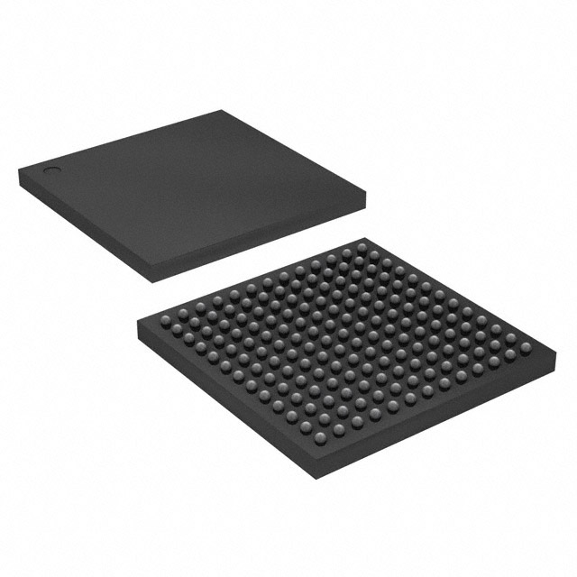
Figure 2: 10M16SAU169I7G in 169-ball UBGA package — top and bottom views of the IC.
5. Application Circuits & Design Guide
The 10M16SAU169I7G is widely deployed in industrial control systems, motor drives, sensor fusion hubs, IoT edge gateways, video surveillance pre-processing, and medical instrumentation. Its integrated dual ADC simplifies mixed-signal designs by eliminating external ADC chips. The single-supply operation (1.2 V core with internal voltage regulation) further reduces power management complexity.
For rapid prototyping, Altera offers the MAX 10 FPGA Development Kit and the popular Terasic DE10-Lite board, both featuring USB-Blaster programming, SDRAM, VGA output, and Arduino-compatible expansion headers. The free Quartus Prime Lite Edition provides synthesis, place-and-route, timing analysis, and JTAG/SPI programming support.

Figure 3: Altera MAX 10 FPGA Development Kit — a reference design platform for evaluating the 10M16SAU169I7G and related MAX 10 devices.
Typical Application Areas
- Industrial Automation: PLC I/O expansion, motor control, sensor aggregation
- IoT Edge Computing: Protocol bridging (Modbus/CAN/SPI to Ethernet), local inference
- Medical Devices: Portable ultrasound front-end, patient monitoring signal processing
- Video & Imaging: Camera interface bridging (MIPI CSI-2 to parallel), image pre-processing
- Test & Measurement: Data acquisition with on-chip ADC, high-speed pattern generation
Video Tutorial: Getting Started with MAX 10 FPGA
6. Frequently Asked Questions (FAQ)
Q1: What is the difference between the 10M16SAU169I7G and the 10M16SAU169C8G?
Both share the same 16K LE die in a 169-UBGA package, but they differ in temperature range and speed grade. The I7G variant is rated for industrial temperature (−40 °C to +100 °C) at speed grade 7, while the C8G is rated for commercial temperature (0 °C to +85 °C) at speed grade 8. Choose the I7G for harsh-environment deployments.
Q2: Does the 10M16SAU169I7G require an external configuration memory?
No. The MAX 10 family features internal configuration flash memory, enabling instant-on operation within milliseconds of power-up. No external EEPROM, SPI flash, or configuration controller is needed, which simplifies the BOM and board layout.
Q3: What development tools are needed for the 10M16SAU169I7G?
You need Quartus Prime Lite Edition (free from Intel/Altera), which supports synthesis, place-and-route, timing analysis, and JTAG programming. For simulation, ModelSim-Intel FPGA Edition is included. For embedded software, the Nios II Software Build Tools allow you to instantiate a soft-core processor inside the FPGA.
Q4: How many ADC channels does the 10M16SAU169I7G provide?
The device features a dual 12-bit ADC running at up to 1 MSPS. Each ADC block has its own dedicated analog input pins, allowing simultaneous sampling of two analog signals. Up to 18 analog input channels can be multiplexed in total, depending on the I/O bank configuration.
Q5: Can the 10M16SAU169I7G interface with DDR3 memory?
Yes. The MAX 10 10M16 supports DDR3, DDR2, LPDDR2, and SRAM external memory interfaces. The built-in hard memory controller IP simplifies timing closure for high-speed memory designs. Supported data rates depend on the speed grade and I/O standard configuration.
Q6: What is the power consumption of the 10M16SAU169I7G?
Static power consumption is typically under 150 mW at 25 °C. Dynamic power depends on the design utilization, clock frequency, and toggle rate. Intel provides the PowerPlay Early Power Estimator spreadsheet and the Quartus Power Analyzer tool for accurate power estimation during the design phase.


