
10M16SAU169I7G Datasheet, Specifications & Application Guide | Altera MAX 10 FPGA
The 10M16SAU169I7G is a non-volatile FPGA from the Altera (Intel) MAX 10 family, built on a 55 nm process node. Featuring 16,000 logic elements, an integrated dual 12-bit ADC, and internal flash configuration memory, this device delivers instant-on operation without external configuration devices. Its industrial-grade temperature rating (−40 °C to +100 °C) and single power-supply design make it ideal for harsh-environment embedded applications.
Table of Contents
- 1. Key Specifications & Parameters
- 2. Block Diagram & Architecture
- 3. Pinout & Package Information
- 4. Application Circuits & Design Guide
- 5. Ordering & Availability
- 6. Frequently Asked Questions (FAQ)
1. Key Specifications & Parameters
The following table summarizes the core electrical and functional parameters of the 10M16SAU169I7G FPGA.
| Parameter | Value |
|---|---|
| Manufacturer | Altera (Intel) |
| Family | MAX 10 |
| Part Number | 10M16SAU169I7G |
| Logic Elements (LEs) | 16,000 |
| Logic Array Blocks (LABs) | 1,000 |
| Embedded RAM (M9K) | 549 Kb |
| User Flash Memory (UFM) | 2,304 Kb |
| DSP Blocks (18×18 Multipliers) | 45 |
| PLLs | 4 |
| ADC | Dual 12-bit, up to 1 MSPS |
| Maximum User I/O Pins | 130 |
| LVDS Pairs | Up to 22 |
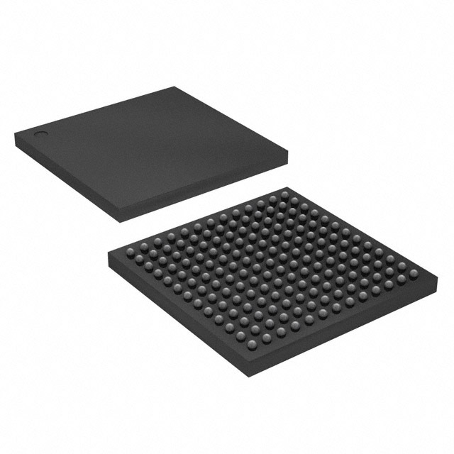
| Package | UBGA-169 (11 mm × 11 mm) |
| Core Voltage | 1.2 V (integrated regulator) |
| I/O Voltage | 3.0 V – 3.3 V |
| Temperature Grade | Industrial (−40 °C to +100 °C) |
| Speed Grade | 7 |
| Process Technology | 55 nm |
| Configuration | Internal flash (instant-on) |
| Power Supply | Single supply (3.3 V input) |
| I/O Standards | LVTTL, LVCMOS, SSTL, HSTL, PCI, LVDS |
| External Memory Support | DDR2, DDR3, LPDDR2, SRAM |
The part number decodes as: 10M16 (MAX 10, 16K LEs) + S (single power supply) + A (analog/ADC enabled) + U169 (UBGA-169 package) + I (industrial temp) + 7 (speed grade) + G (lead-free/RoHS).
2. Block Diagram & Architecture
The MAX 10 architecture integrates logic elements, M9K embedded memory blocks, DSP multiplier blocks, four fabric PLLs, a dual 12-bit ADC, and user flash memory on a single monolithic die. The internal configuration flash eliminates the need for external configuration devices, enabling instant-on operation within milliseconds of power-up.
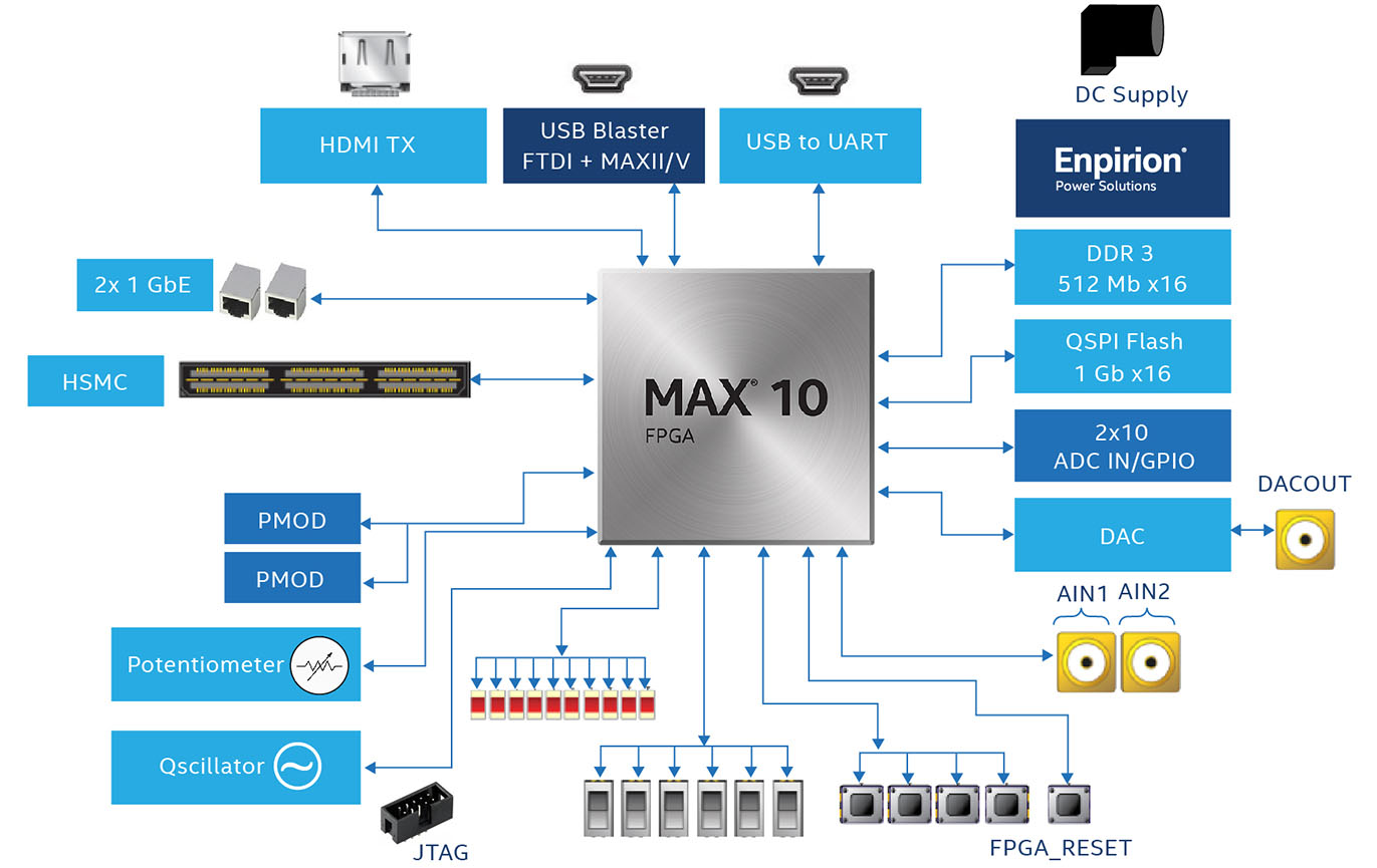
Each Logic Array Block (LAB) contains 16 logic elements, where each LE provides a four-input look-up table (LUT), a programmable register, and carry chain logic. The 45 embedded 18×18 multiplier blocks accelerate DSP-intensive tasks such as digital filtering and motor control algorithms.
3. Pinout & Package Information
The 10M16SAU169I7G is housed in a 169-ball Ultra-thin Fine-pitch Ball Grid Array (UBGA) package measuring 11 mm × 11 mm with a 0.8 mm ball pitch. This compact footprint supports up to 130 user I/O pins and 22 LVDS differential pairs, providing ample connectivity for multi-sensor and multi-protocol industrial designs.
The single power-supply variant simplifies PCB design by requiring only a 3.3 V input, with the 1.2 V core voltage generated by an on-chip integrated voltage regulator. Pin-out files in PDF, XLS, and TXT formats are available from Intel's official Altera pin-out resources page.
4. Application Circuits & Design Guide
The 10M16SAU169I7G is widely deployed in industrial control systems, motor drives, sensor hub aggregation, IoT edge gateways, video surveillance pre-processing, and medical instrumentation. The integrated dual 12-bit ADC eliminates external ADC components, reducing BOM cost and board space in mixed-signal designs.
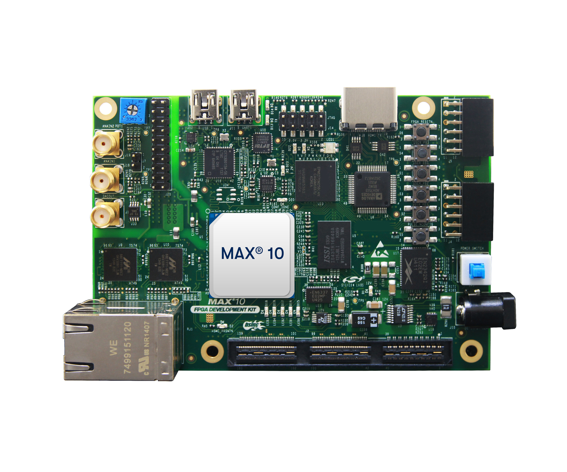
For rapid prototyping, Altera offers the MAX 10 FPGA Development Kit featuring on-board USB-Blaster II programming, DDR3 SDRAM, HSMC expansion, HDMI output, and dual Ethernet interfaces. The popular Terasic DE10-Lite board provides a lower-cost alternative with Arduino-compatible headers, VGA output, and an on-board accelerometer.
Recommended Design Resources
- Quartus Prime Lite Edition — Free synthesis and programming tool for MAX 10 devices
- Platform Designer (Qsys) — System integration tool for connecting IP cores
- ModelSim-Intel Edition — RTL simulation for functional verification
- Nios II Soft Processor — Embedded processor core for software-defined control
5. Ordering & Availability
The 10M16SAU169I7G is available from authorized distributors worldwide. Check current stock and pricing at wwdparts.com for competitive quotes and fast shipping. Related MAX 10 variants you may also consider:
- 10M16SAU169C8G — Commercial temperature grade (0 °C to +85 °C)
- 10M08SAU169 — 8K LE variant in the same U169 package
- Browse all MAX 10 FPGA devices
6. Frequently Asked Questions (FAQ)
What is the 10M16SAU169I7G?
The 10M16SAU169I7G is a non-volatile FPGA from the Altera (Intel) MAX 10 family. It integrates 16,000 logic elements, 549 Kb of embedded SRAM, 2,304 Kb of user flash memory, 45 DSP blocks, a dual 12-bit ADC, and 4 PLLs in a compact UBGA-169 package. It is rated for industrial temperatures (−40 °C to +100 °C) with speed grade 7.
Does the 10M16SAU169I7G require an external configuration device?
No. The MAX 10 family features internal flash-based configuration memory, enabling instant-on operation within milliseconds of power-up. This eliminates the need for external serial configuration ROMs or JTAG-only programming flows, reducing BOM cost and simplifying board layout.
What power supply voltage does the 10M16SAU169I7G need?
The 10M16SAU169I7G uses a single 3.3 V power supply. The device includes an integrated voltage regulator that generates the 1.2 V core voltage internally, significantly simplifying power supply design for space-constrained applications.
What are the main applications of the 10M16SAU169I7G?
Common applications include industrial control and automation, motor drive controllers, multi-sensor hubs, IoT edge gateways, video surveillance pre-processing, medical instrumentation, and portable test equipment. The integrated ADC makes it particularly suited for mixed-signal designs that require analog-to-digital conversion.
What is the difference between 10M16SAU169I7G and 10M16SAU169C8G?
Both share the same 16K LE logic fabric, memory, and package. The key differences are: the "I7G" variant is rated for industrial temperatures (−40 °C to +100 °C) with speed grade 7, while the "C8G" variant is rated for commercial temperatures (0 °C to +85 °C) with speed grade 8. Choose the I7G for extended temperature environments and the C8G for cost-optimized commercial designs.
What software tools are needed to program the 10M16SAU169I7G?
You need Intel Quartus Prime Lite Edition (free download) for synthesis, place-and-route, and device programming. ModelSim-Intel Edition handles RTL simulation. Platform Designer (formerly Qsys) enables system-level integration of IP cores. Programming is done via USB-Blaster or USB-Blaster II JTAG cables.


