
10M16SAU169I7G Datasheet, Pinout & Specs — Altera MAX 10 FPGA
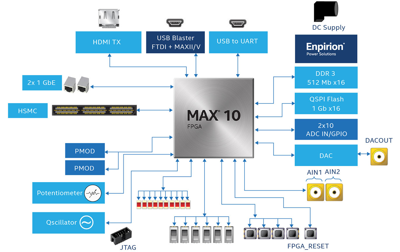
The 10M16SAU169I7G is a non-volatile FPGA from the Altera (Intel) MAX 10 family, fabricated on a 55 nm process with integrated flash configuration memory. Offering 16,000 logic elements, 549 Kb of embedded SRAM, 2,304 Kb of user flash memory (UFM), a dual 12-bit ADC, and 4 PLLs, it provides instant-on operation with no external configuration device required. The device ships in a compact 169-ball UBGA package with an industrial temperature rating of −40 °C to +100 °C and a speed grade of 7, making it ideal for space-constrained, mixed-signal industrial applications.
What Is the 10M16SAU169I7G?
The 10M16SAU169I7G belongs to the MAX 10 family — Altera's single-chip, non-volatile FPGA line built on TSMC's 55 nm embedded-flash process. The "non-volatile" designation means the configuration bitstream is stored in on-die flash memory, enabling the device to power up and begin operating in under 10 ms without an external configuration ROM or processor. This instant-on behavior is critical for applications such as motor-drive pre-drivers, power-supply sequencers, and safety interlock logic where the FPGA must be functional before upstream processors complete their boot sequence.
The part number decodes as follows: 10M16 = MAX 10 with 16,000 logic elements, S = single power-supply mode (internal voltage regulator generates 1.2 V core from a 3.3 V input), A = analog block enabled (dual 12-bit ADC), U169 = 169-ball UBGA package, I = industrial temperature (−40 °C to +100 °C), and 7 = speed grade 7. Internally the device organizes its 16,000 logic elements into 1,000 Logic Array Blocks (LABs), each containing 16 look-up-table-based LEs with configurable registers. Embedded memory consists of M9K blocks (each 9,216 bits of true dual-port SRAM), totaling 549 Kb of on-chip storage usable as RAM, ROM, FIFO, or shift register.
Pinout Configuration and Packaging
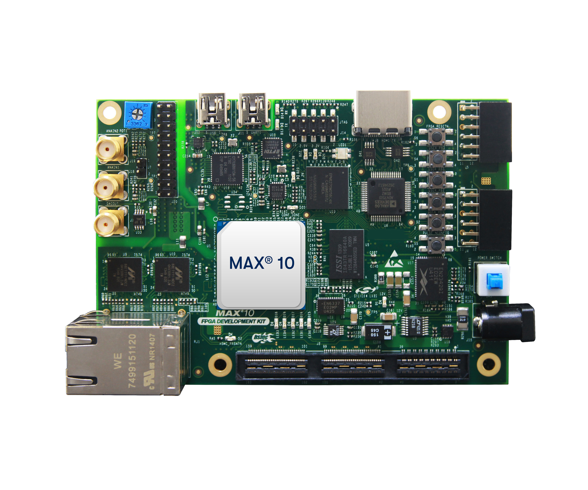
The 10M16SAU169I7G is housed in a 169-ball Ultra-thin Fine-pitch BGA (UBGA) package measuring approximately 11 × 11 mm with a 0.8 mm ball pitch. Of the 169 balls, up to 130 are available as general-purpose I/O pins distributed across 8 I/O banks. Each I/O bank supports independent VCCIO supply rails, allowing mixed-voltage interfacing at 1.2 V, 1.5 V, 1.8 V, 2.5 V, or 3.3 V within a single device. The package supports up to 22 LVDS differential pairs for high-speed parallel data transfer.
In single power-supply mode (the "S" variant), only a 3.3 V input is required — the on-chip voltage regulator generates the 1.2 V core supply internally. This significantly reduces BOM cost and simplifies board layout. Critical pins include dedicated JTAG ports (TCK, TDI, TDO, TMS) for programming and debug, analog input pins (ANAIN1, ANAIN2) for the dual ADC, and MSEL pins for configuration mode selection. The device supports dual-image flash configuration, enabling fail-safe remote firmware updates where a golden image can be retained as fallback.

Specifications Parameter Table
| Specification | Technical Details |
|---|---|
| Device Family | MAX 10 (Altera / Intel) |
| Logic Elements (LEs) | 16,000 |
| Logic Array Blocks (LABs) | 1,000 |
| Embedded SRAM | 549 Kb (M9K blocks) |
| User Flash Memory (UFM) | 2,304 Kb |
| Analog-to-Digital Converter | Dual 12-bit SAR ADC, up to 1 MSPS per channel |
| PLLs | 4 (fabric and I/O phase-locked loops) |
| Global Clock Networks | 20 |
| User I/O Pins (U169) | 130 |
| LVDS Pairs (U169) | Up to 22 |
| DSP Blocks | Embedded multipliers (18 × 18) |
| Package | 169-UBGA, 11 × 11 mm, 0.8 mm pitch |
| Process Node | 55 nm (TSMC embedded flash) |
| Core Voltage | 1.2 V (internally regulated from 3.3 V in S-variant) |
| I/O Voltage | 1.2 V / 1.5 V / 1.8 V / 2.5 V / 3.3 V (per-bank) |
| Speed Grade | 7 (Industrial) |
| Temperature Range | −40 °C to +100 °C (Industrial) |
| I/O Standards | 3.0 V / 3.3 V LVTTL, 1.0 V–3.3 V LVCMOS, SSTL, HSTL, HSUL, LVDS, PCI |
| Configuration | Internal flash (instant-on), dual-image support, JTAG |
| External Memory Support | DDR2, DDR3, LPDDR2, SRAM (soft controller) |
| RoHS / Lead-Free | Yes |
Typical Applications and Circuit Considerations
The 10M16SAU169I7G excels in applications demanding a compact, single-chip mixed-signal solution with instant-on capability. The integrated dual 12-bit ADC eliminates external ADC ICs for sensor monitoring, while the non-volatile flash configuration removes the need for external EEPROM or flash memory. Typical system-level applications include:
- Industrial Sensor Hubs and IoT Edge Nodes: The on-chip ADC directly digitizes analog sensor outputs (temperature, pressure, current) while the FPGA fabric implements real-time filtering, threshold detection, and communication protocol engines (SPI, I²C, UART). The industrial temperature rating ensures reliable operation in factory-floor environments.
- Motor Drive Pre-Drivers and Power Management: Instant-on operation allows the FPGA to control power sequencing and motor pre-driver logic before the main processor boots. The ADC monitors bus voltages and phase currents in real time for closed-loop control.
- Video Surveillance Pre-Processing: M9K memory blocks serve as line buffers for image pre-processing pipelines (Bayer demosaicing, histogram equalization) before data is forwarded to a host SoC over parallel or serial interfaces.
- Medical Instrumentation: Portable diagnostic equipment leverages the small UBGA footprint, single-supply operation, and ADC for bio-signal acquisition chains (ECG, pulse oximetry front-ends) with FPGA-based digital filtering.
For board design, the single power-supply "S" variant requires only a well-filtered 3.3 V rail — the internal regulator generates 1.2 V core voltage. Altera recommends 100 nF MLCC decoupling capacitors on every VCC pin pair, plus 10 µF bulk capacitors per supply domain. The ADC analog inputs should be routed as short, guarded traces with ground shielding to minimize noise coupling. For the UBGA package, a 4-layer PCB stackup with dedicated power and ground planes is recommended, and all unused I/O pins should be driven low or left as tri-state inputs with internal pull-down resistors enabled.
Video: Getting Started with Intel MAX 10 FPGA
Equivalents, Cross-Reference, and Lifecycle
The 10M16SAU169I7G carries an Active lifecycle status as of 2026, with no Product Discontinuation Notice (PDN) issued by Altera/Intel. The MAX 10 family remains in volume production and is widely stocked by major distributors including DigiKey, Mouser, Arrow, and Farnell.
Within the MAX 10 family, the closest pin-compatible variants in the same U169 package are:
- 10M16SAU169C8G — same die, commercial temperature grade (0 °C to 85 °C), C8 speed grade. Drop-in replacement for non-industrial environments.
- 10M08SAU169I7G — 8,000 logic elements in the same U169 package, industrial grade. Pin-compatible downgrade for designs requiring less logic capacity.
- 10M16SAU169A7G — same logic capacity and package, but "A" (automotive-qualified) variant for ADAS and in-vehicle applications.
Cross-family migration paths:
- Lattice MachXO3LF (LCMXO3LF-6900C): Non-volatile FPGA with 6,900 LUTs, instant-on, and integrated flash — a lower-density alternative with similar single-chip philosophy.
- Microchip PolarFire (MPF100T): 28nm flash-based FPGA with 100K LEs, 12.7 Gbps transceivers, and non-volatile configuration for designs needing a growth path.
- Xilinx Spartan-7 (XC7S25): 28nm SRAM-based FPGA with 23,360 logic cells — requires external flash but offers a Vivado-based design flow alternative.
For engineers evaluating related MAX 10 devices, see also our technical guides on the 10M16SAU169C8G, the 10M04SCE144C8G, and the 10M08SAE144C8G.
Frequently Asked Questions (FAQ)
What is the 10M16SAU169I7G and what family does it belong to?
The 10M16SAU169I7G is a non-volatile FPGA from the Altera (Intel) MAX 10 family, built on a 55 nm embedded-flash process. It integrates 16,000 logic elements, 549 Kb of embedded SRAM, a dual 12-bit ADC, 4 PLLs, and internal flash configuration memory into a single chip, enabling instant-on operation without external configuration devices.
What package does the 10M16SAU169I7G use and how many I/O pins does it have?
The 10M16SAU169I7G is packaged in a 169-ball UBGA (Ultra-thin Fine-pitch Ball Grid Array) measuring 11 × 11 mm with 0.8 mm ball pitch. It provides up to 130 user I/O pins across 8 I/O banks and supports up to 22 LVDS differential pairs. Each bank has an independent VCCIO rail supporting 1.2 V to 3.3 V interfaces.
Does the 10M16SAU169I7G require an external power supply regulator?
No. The "S" in the part number indicates single power-supply mode with an integrated voltage regulator. You only need to supply 3.3 V — the device internally generates the 1.2 V core voltage. This eliminates the need for a separate 1.2 V regulator, reducing BOM cost and board space. VCCIO rails for I/O banks must still be supplied at the desired voltage levels.
What are the ADC specifications of the 10M16SAU169I7G?
The 10M16SAU169I7G integrates a dual-channel 12-bit successive-approximation-register (SAR) ADC with up to 1 MSPS sampling rate per channel. The ADC supports both dedicated analog input pins and internal temperature sensor monitoring. It features a configurable analog multiplexer that can route multiple external analog signals to the ADC channels, enabling multi-sensor monitoring with minimal external circuitry.
What design software do I need to program the 10M16SAU169I7G?
The 10M16SAU169I7G is fully supported by Intel Quartus Prime Lite Edition, which is free with no license key required. The tool chain provides synthesis, place-and-route, timing analysis, and JTAG programming for all MAX 10 devices. The design flow supports Verilog, SystemVerilog, and VHDL, along with Platform Designer for system integration and Nios II soft processor support.
What is the operating temperature range and can it be used in industrial environments?
Yes, the 10M16SAU169I7G is rated for the full industrial temperature range of −40 °C to +100 °C (indicated by the "I" suffix). This makes it suitable for factory automation, outdoor IoT deployments, motor control, and other demanding environments. The commercial variant (10M16SAU169C8G) operates from 0 °C to 85 °C for less stringent applications.


