
10M16SAU169I7G Datasheet, Pinout & Specifications – Intel (Altera) MAX 10 FPGA Complete Guide
The 10M16SAU169I7G is a high-performance FPGA from the Intel (Altera) MAX 10 family, built on 55nm non-volatile process technology. Featuring 16,000 logic elements, an integrated ADC, and user flash memory in a compact 169-UBGA package, this industrial-grade device is designed for cost-sensitive embedded applications requiring instant-on functionality and single-chip solutions. This comprehensive guide covers its datasheet specifications, pinout, block diagram, and real-world application circuits.
Table of Contents
- Overview & Key Features
- Detailed Specifications & Parameters
- Block Diagram & Architecture
- Pinout & Package Information
- Application Circuits & Design Examples
- Frequently Asked Questions
Overview & Key Features
The 10M16SAU169I7G belongs to the Intel MAX 10 FPGA family, the industry's first single-chip, non-volatile FPGA with integrated analog functionality. Unlike traditional FPGAs that require external configuration memory, the MAX 10 integrates dual configuration flash, enabling instant-on operation within milliseconds of power-up. This makes it ideal for applications where boot time is critical, such as industrial control systems and automotive electronics.
Key advantages of the 10M16SAU169I7G include its integrated dual analog-to-digital converters (ADC), up to 156 KB of user flash memory for data storage, and support for DDR3 external memory interfaces. The "I7G" suffix indicates industrial temperature range (-40°C to +100°C) and speed grade 7, suitable for harsh operating environments. For engineers seeking related MAX 10 FPGA options, see our guide on the 10M16SAU169C8G (commercial grade variant).
Detailed Specifications & Parameters
| Parameter | Value |
|---|---|
| Part Number | 10M16SAU169I7G |
| Manufacturer | Intel (Altera) |
| Family | MAX 10 (10M16) |
| Logic Elements (LEs) | 16,000 |
| Logic Array Blocks (LABs) | 1,000 |
| Embedded Memory (M9K) | 549 Kb (562,176 bits) |
| 18×18 Multipliers | 45 |
| Phase-Locked Loops (PLLs) | 2 (on U169 package) |
| Analog-to-Digital Converter | Dual ADC (up to 1 MSPS, 12-bit) |
| User Flash Memory | Up to 156 KB |
| User I/O Pins | 130 |
| I/O Standards | 3.3V LVTTL, LVCMOS, SSTL, HSTL, HSUL, LVDS |
| External Memory Interface | DDR2, DDR3, LPDDR2, SRAM |
| Configuration | Internal dual flash (instant-on) |
| Bitstream Security | AES 128-bit encryption |
| Core Voltage | 1.2V |
| I/O Supply Voltage | 2.85V – 3.465V (3.3V nominal) |
| Operating Temperature | -40°C to +100°C (Industrial) |
| Speed Grade | 7 |
| Process Technology | 55nm |
| Package | 169-UBGA (11mm × 11mm) |
| Mounting | Surface Mount (SMD/SMT) |
| RoHS | Compliant |
The 45 embedded 18×18 multipliers enable efficient DSP operations, making the 10M16SAU169I7G suitable for signal processing tasks without consuming programmable logic resources. For comparison with smaller MAX 10 devices, check out the 10M08SAE144C8G (8K LE variant).
Block Diagram & Architecture
The MAX 10 architecture centers around an array of Logic Array Blocks (LABs), each containing 16 Adaptive Logic Modules (ALMs). The 10M16SAU169I7G organizes 1,000 LABs in a grid interconnected by row and column routing resources, with M9K embedded memory blocks distributed throughout the fabric.

Figure 1: MAX 10 FPGA development kit block diagram illustrating the core architecture and peripheral connectivity.
The dual ADC blocks are hardened IP located at the device periphery, each capable of 1 MSPS sampling at 12-bit resolution. The two PLLs available on the U169 package provide flexible clock synthesis and management with frequency multiplication, division, and phase shifting capabilities. Global clock networks distribute clocks across the entire device with minimal skew.
Pinout & Package Information
The 10M16SAU169I7G uses a 169-ball UBGA (Ultra Fine-pitch Ball Grid Array) package measuring 11mm × 11mm with 0.8mm ball pitch. Of the 169 balls, 130 are available as user I/O pins organized into multiple I/O banks supporting different voltage standards simultaneously.
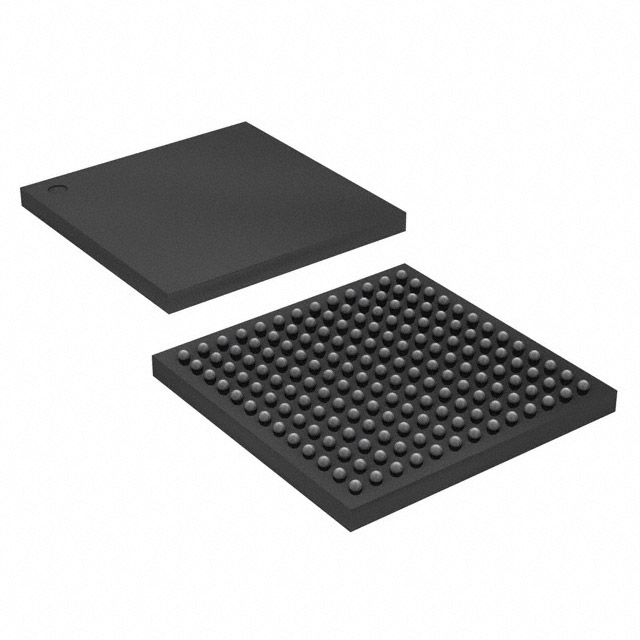
Figure 2: 10M16SAU169I7G in 169-UBGA package – compact 11×11mm BGA footprint ideal for space-constrained designs.
The I/O banks support a wide range of single-ended and differential standards including 3.3V LVTTL, 1.2V–3.3V LVCMOS, SSTL-15, HSTL-12, and LVDS. Each I/O bank can be independently powered, allowing designers to interface with multiple voltage domains on a single chip. Dedicated configuration pins handle JTAG programming and internal flash configuration.
Application Circuits & Design Examples
The 10M16SAU169I7G excels in a variety of embedded applications due to its integrated flash, ADC, and instant-on capability. Common use cases include industrial automation controllers, motor drive interfaces, sensor hubs in IoT gateways, protocol bridges, and LED display controllers.

Figure 3: MAX 10 FPGA development kit – a complete reference platform demonstrating DDR3 memory, ADC input, and multi-protocol I/O connectivity.
A typical design pairs the 10M16SAU169I7G with DDR3 SDRAM for data buffering, a 3.3V regulated supply, and JTAG header for programming. The internal dual configuration flash eliminates the need for external EEPROM/flash, reducing BOM cost and PCB area. The integrated ADC can directly digitize sensor signals, removing the need for external ADC ICs in mixed-signal applications. For a deeper look at FPGA design workflows, see our 10M04SCE144C8G design guide.
Video Tutorial: Getting Started with MAX 10 FPGA
Watch: Introduction to MAX 10 FPGA development with Intel Quartus Prime.
Frequently Asked Questions
What is the difference between 10M16SAU169I7G and 10M16SAU169C8G?
The primary differences are temperature grade and speed grade. The 10M16SAU169I7G is an industrial-grade device operating from -40°C to +100°C with speed grade 7, while the 10M16SAU169C8G is a commercial-grade device rated for 0°C to +85°C with speed grade 8. The industrial variant is preferred for harsh environments, while the commercial variant offers slightly different timing characteristics.
Does the 10M16SAU169I7G require external configuration memory?
No. The MAX 10 FPGA integrates dual configuration flash memory on-chip, supporting instant-on operation. The device configures itself from internal flash within milliseconds of power-up, eliminating the need for external EEPROM or flash memory ICs. This also enables dual-image storage for safe remote firmware updates.
What development tools are needed for the 10M16SAU169I7G?
The 10M16SAU169I7G is supported by Intel Quartus Prime Lite Edition (free) or Quartus Prime Standard Edition. Design entry supports Verilog, VHDL, and schematic capture. A USB-Blaster or USB-Blaster II programmer is needed for JTAG programming. Evaluation boards like the DE10-Lite or MAX 10 FPGA Evaluation Kit provide a ready-to-use development platform.
How many ADC channels does the 10M16SAU169I7G have?
The 10M16SAU169I7G features dual ADC blocks, each with up to 9 analog input channels (depending on the device variant and package). Each ADC supports 12-bit resolution at up to 1 MSPS (mega samples per second). The ADCs can be used for temperature sensing, voltage monitoring, or direct sensor digitization, reducing external component requirements.
What is the maximum DDR3 memory speed supported by the 10M16SAU169I7G?
The MAX 10 FPGA family supports DDR3 SDRAM interfaces at up to 300 MHz (600 Mbps data rate). The hard memory controller IP is not available in MAX 10, so DDR3 interfaces use soft memory controller IP implemented in the FPGA fabric. The U169 package provides sufficient I/O pins for a 16-bit DDR3 interface with address and control signals.
Can I use the 10M16SAU169I7G for motor control applications?
Yes, the 10M16SAU169I7G is well-suited for motor control. Its 45 embedded 18×18 multipliers can implement PID controllers and FOC (Field-Oriented Control) algorithms efficiently. The integrated ADC can directly sample motor current and voltage feedback signals, while the industrial temperature rating ensures reliable operation in factory environments. Intel provides reference designs for industrial motor drive applications using MAX 10 FPGAs.


