
Overview of the 10M16SAU169C8G
The 10M16SAU169C8G is a non-volatile FPGA from Intel's (formerly Altera) MAX 10 family, fabricated on a 55 nm process node. It delivers 16,000 logic elements in a compact 169-pin UBGA package (11×11 mm), making it an ideal single-chip solution for industrial control, motor drives, I/O expansion, and sensor-hub applications. Thanks to its integrated dual-configuration flash, user flash memory, and analog-to-digital converter, designers can eliminate external configuration devices and discrete ADCs, reducing both board area and BOM cost.
As a member of the MAX 10 series, the 10M16SAU169C8G supports instant-on operation with a configuration time of less than 10 ms, enabling deterministic system start-up. The device is fully supported by Intel's Quartus Prime Lite Edition—a free-to-use design suite—and is pin-compatible with other MAX 10 variants in the U169 package, giving engineers a clear migration path as design requirements evolve.
Key Specifications & Parameters
| Parameter | Value |
|---|---|
| Part Number | 10M16SAU169C8G |
| Manufacturer | Intel (Altera) |
| Family | MAX 10 FPGA |
| Logic Elements (LEs) | 16,000 |
| Logic Array Blocks (LABs) | 1,000 |
| Embedded Memory (M9K) | 549 Kb |
| Total RAM Bits | 562,176 |
| User Flash Memory | Integrated (up to 336 Kb) |
| 18×18 Embedded Multipliers | 45 |
| PLLs | 4 |
| User I/O Pins | 130 |
| Max LVDS Pairs | 22 |
| ADC Blocks | 1 (dual 12-bit, 1 MSPS) |
| Package | 169-UBGA (11×11 mm, 0.8 mm pitch) |
| Supply Voltage (VCCINT) | 1.2 V |
| I/O Voltage Range | 1.0 V – 3.3 V |
| Speed Grade | C8 (commercial) |
| Operating Temperature | 0 °C to 85 °C (TJ) |
| Process Technology | 55 nm |
| Configuration | Internal dual-configuration flash |
| External Memory Interface | DDR3, DDR3L, DDR2, LPDDR2 |
| Bitstream Security | AES-256 encryption |
Block Diagram & Architecture
The MAX 10 architecture integrates logic, memory, DSP, ADC, and flash blocks onto a single die. The diagram below illustrates the functional blocks and their interconnections within the 10M16SAU169C8G evaluation ecosystem.
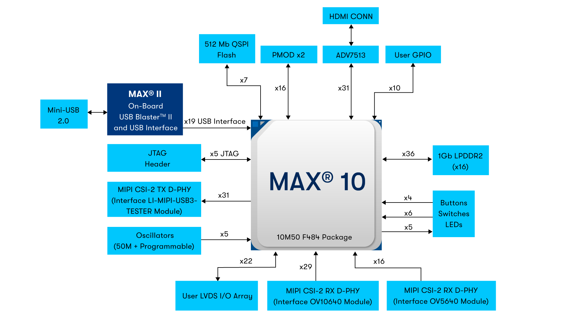
Key architectural highlights include four analog PLLs for flexible clock synthesis, 45 embedded 18×18 multipliers for DSP-intensive workloads, and an integrated 12-bit SAR ADC that supports up to 18 analog input channels with a 1 MSPS sample rate.
Pinout & Package Information
The 10M16SAU169C8G uses a 169-ball UBGA package measuring 11×11 mm with a 0.8 mm ball pitch. The compact form factor makes it well-suited for space-constrained designs while still providing 130 user-configurable I/O pins supporting voltage levels from 1.0 V to 3.3 V LVCMOS and LVTTL standards.

The pin map organizes I/O into banks that share a common VCCIO rail. Each bank can independently target different I/O standards, allowing mixed-voltage interfacing. Differential I/O pairs support LVDS, mini-LVDS, RSDS, and sub-LVDS signaling for high-speed serial links.
Application Circuit & Design Guide
Below is the MAX 10 evaluation kit board, which demonstrates a reference design for the 10M16SAU169C8G and related MAX 10 devices. It showcases typical connectivity including JTAG programming, power regulation, external memory interfaces, and on-board debug headers.
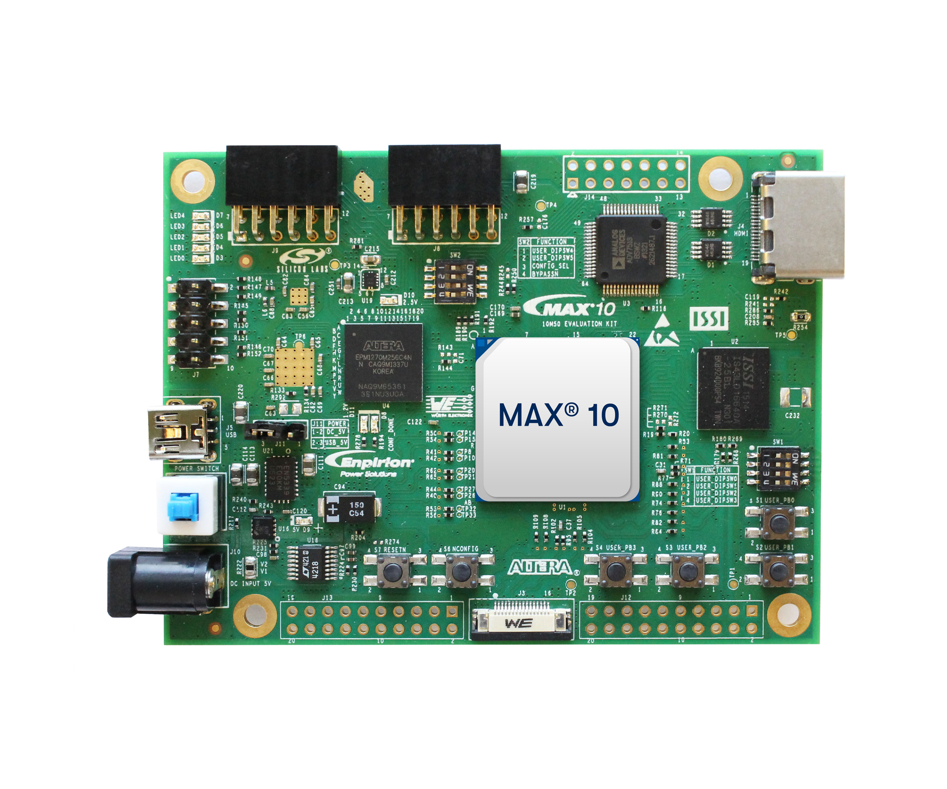
For a minimal design, the 10M16SAU169C8G requires decoupling capacitors on each VCC and VCCIO pin, a 3.3 V regulated supply, and a JTAG connection for programming. The internal flash eliminates the need for an external configuration PROM. A Nios II soft processor can be instantiated for embedded-control tasks, combining FPGA flexibility with MCU-like programmability in a single device.
Typical Application Areas
- Industrial Automation – Motor control, sensor fusion, PLC I/O modules
- Communications – Protocol bridging, control-plane processing, PHY-layer interfacing
- Medical Devices – Portable imaging, patient monitoring front-ends
- Consumer Electronics – LED display controllers, audio/video processing
- Automotive – ADAS sensor hubs, in-vehicle networking gateways
Video Tutorial
Frequently Asked Questions
What is the 10M16SAU169C8G?
The 10M16SAU169C8G is a non-volatile FPGA from Intel's MAX 10 family. It contains 16,000 logic elements, 549 Kb of embedded SRAM, an integrated 12-bit ADC, and internal dual-configuration flash, all housed in a 169-ball UBGA package.
What package does the 10M16SAU169C8G use?
It uses a 169-pin Ultra-Thin Fine-Pitch BGA (UBGA) package measuring 11×11 mm with a 0.8 mm ball pitch. The package is RoHS-compliant and uses lead-free solder balls (indicated by the "G" suffix in the ordering code).
Does the 10M16SAU169C8G need an external configuration memory?
No. The MAX 10 family features internal dual-configuration flash, so no external EEPROM or serial flash is required. This also enables instant-on operation with configuration times below 10 ms.
What design software supports the 10M16SAU169C8G?
Intel Quartus Prime Lite Edition (free) fully supports all MAX 10 devices including the 10M16SAU169C8G. It provides synthesis, place-and-route, timing analysis, and the Platform Designer (Qsys) system integration tool.
Can I use the integrated ADC for analog signal acquisition?
Yes. The 10M16SAU169C8G includes a 12-bit SAR ADC with up to 1 MSPS throughput and support for up to 18 single-ended analog input channels. It includes an internal temperature-sensing diode and can be controlled via a soft-IP ADC Toolkit in Quartus Prime.
What is the difference between 10M16SAU169C8G and 10M16SAU169I7G?
Both share the same 16K-LE die and U169 package. The key differences are temperature grade and speed: the C8G is a commercial-grade device rated 0–85 °C with speed grade 8, while the I7G is an industrial-grade device rated −40 °C to 100 °C with the faster speed grade 7.


