
Overview of the 10M16SAU169I7G MAX 10 FPGA
The 10M16SAU169I7G is a non-volatile FPGA from the Intel (formerly Altera) MAX 10 family. Built on a 55 nm flash-based process, this device integrates 16,000 logic elements, an analog-to-digital converter (ADC), user flash memory, and up to 549 Kb of embedded SRAM into a compact 169-ball UBGA package. Unlike SRAM-based FPGAs, the MAX 10 stores its configuration internally, eliminating the need for an external configuration device and enabling instant-on operation. The industrial-grade "I7G" variant operates across the extended −40 °C to +100 °C temperature range, making it suitable for harsh-environment deployments.
Designers choose the 10M16SAU169I7G for single-chip solutions that combine programmable logic with analog and memory functions, reducing board space, BOM cost, and power consumption compared to multi-chip alternatives. It is widely used in industrial automation, motor control, sensor aggregation, and embedded IoT gateways. You can source this part and similar components at wwdparts.com.
Key Specifications & Parameters
| Parameter | Value |
|---|---|
| Part Number | 10M16SAU169I7G |
| Manufacturer | Altera (Intel) |
| Family | MAX 10 (10M16) |
| Logic Elements (LEs) | 16,000 |
| Logic Array Blocks (LABs) | ~1,000 |
| Embedded Memory | 549 Kb (M9K blocks) |
| User Flash Memory (UFM) | Yes (internal, non-volatile) |
| 18×18 Multipliers (DSP) | Yes |
| PLLs | 4 |
| ADC | Yes (12-bit, dual SAR) |
| Max User I/O (U169) | 130 |
| LVDS Pairs | Up to 22 |
| Package | UBGA-169 (11 × 11 mm) |
| Core Voltage | 1.2 V |
| I/O Voltage | 1.0 V – 3.3 V (multi-standard) |
| Operating Temperature | −40 °C to +100 °C (Industrial) |
| Speed Grade | 7 |
| Process Technology | 55 nm Flash |
| Configuration | Internal (instant-on, dual-image boot) |
| External Memory Support | DDR2, DDR3, LPDDR2, SRAM |
| I/O Standards | LVTTL, LVCMOS, SSTL, HSTL, HSUL, PCI, Differential |
| RoHS / Lead-Free | Yes |
For competitive pricing and stock availability, check the wwdparts.com FPGA catalog.
Pinout Diagram & Package Information
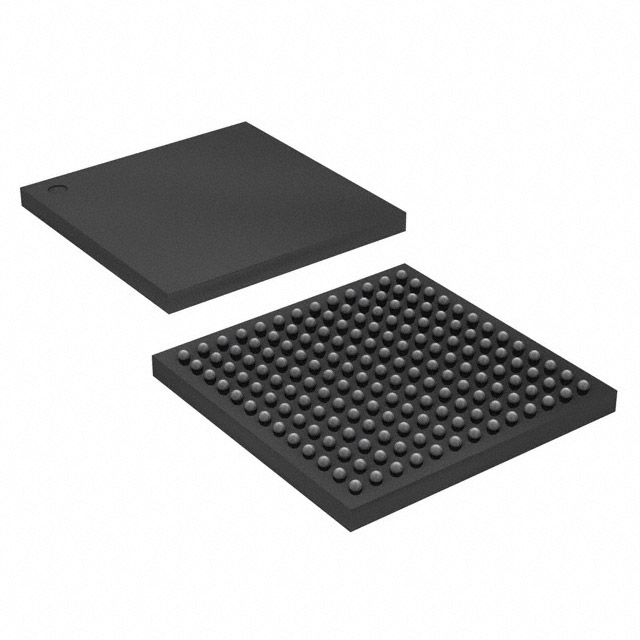
The 10M16SAU169I7G comes in a 169-ball Ultra Fine-pitch Ball Grid Array (UBGA) package measuring 11 × 11 mm with a 0.8 mm ball pitch. The U169 package provides 130 user I/O pins organized across multiple I/O banks supporting a wide range of single-ended and differential signaling standards. The compact footprint makes it ideal for space-constrained PCB designs.
Key pin groups include VCCIO (I/O power banks), VCCINT (1.2 V core), GND, JTAG (TCK/TMS/TDI/TDO), configuration pins (nCONFIG, nSTATUS, CONF_DONE), analog input channels for the ADC, and clock input pins routed to the internal PLLs. Consult the official Intel MAX 10 pin-out file for the complete ball map.
Block Diagram & Internal Architecture
The MAX 10 architecture integrates several major functional blocks on a single die. The core fabric consists of Logic Array Blocks (LABs), each containing Adaptive Logic Modules (ALMs) that implement combinational and sequential logic. Surrounding the logic core are embedded M9K memory blocks totaling 549 Kb, 18×18 multiplier blocks for DSP functions, and four general-purpose PLLs for clock management.

A distinguishing feature of the MAX 10 is its integrated flash-based configuration memory, supporting dual-image boot with automatic fallback. The on-chip User Flash Memory (UFM) can store application data without an external EEPROM. The 12-bit dual SAR ADC accepts up to 18 analog input channels, enabling direct sensor interfacing without additional components. The I/O ring supports multi-standard voltage levels from 1.0 V to 3.3 V, with up to 22 LVDS pairs for high-speed serial links.
Typical Applications & Design Examples
The 10M16SAU169I7G is a versatile single-chip solution deployed in a wide range of embedded systems:
- Industrial Automation & Motor Control – PWM generation, encoder feedback processing, and real-time control loops using the on-chip DSP blocks.
- Sensor Aggregation & Condition Monitoring – The built-in ADC directly samples temperature, voltage, and current sensors, reducing external component count.
- Embedded IoT Gateways – Protocol bridging (SPI, I2C, UART, Ethernet) with programmable logic and non-volatile data storage in UFM.
- Automotive Infotainment & ADAS – Video processing pipelines and display interfaces leveraging LVDS and DDR3 memory support.
- Consumer Electronics – LED panel drivers, audio DSP, and human-machine interface controllers.
- Test & Measurement – Data acquisition front-ends with the ADC and high-speed I/O capabilities.

The MAX 10 FPGA Development Kit shown above provides a complete hardware platform with Gigabit Ethernet, HDMI, USB-UART, HSMC connectors, and analog inputs for rapid prototyping. Design entry is done through the free Quartus Prime Lite edition supporting Verilog, VHDL, and schematic capture. Browse more FPGA development tools at wwdparts.com engineering blog.
Frequently Asked Questions (FAQ)
What is the 10M16SAU169I7G and what family does it belong to?
The 10M16SAU169I7G is a non-volatile FPGA belonging to the Intel (Altera) MAX 10 family. It features 16,000 logic elements, an integrated ADC, user flash memory, and 549 Kb embedded SRAM in a 169-ball UBGA package. The “I7G” suffix indicates industrial temperature range (−40 °C to +100 °C) and speed grade 7.
Does the 10M16SAU169I7G require an external configuration memory?
No. The MAX 10 FPGA stores its configuration in on-chip flash memory, providing instant-on capability without an external configuration PROM or flash chip. It also supports dual-image boot for remote update with automatic fallback to a known-good image.
What analog features does the 10M16SAU169I7G offer?
The device integrates a 12-bit dual successive-approximation-register (SAR) ADC that can sample up to 18 analog input channels at up to 1 MSPS. This allows direct connection to temperature sensors, voltage dividers, and other analog signals without requiring a separate ADC IC.
What development software is used for the 10M16SAU169I7G?
The 10M16SAU169I7G is supported by Intel Quartus Prime Lite Edition, which is free to download and use. It supports design entry via Verilog, VHDL, or schematic capture, and includes the Platform Designer (formerly Qsys) system integration tool and the Nios II soft processor.
What package options are available for the MAX 10 10M16 device?
The 10M16 device is available in several packages: E144 (EQFP-144), U169 (UBGA-169), U324 (UBGA-324), F256 (FBGA-256), and F484 (FBGA-484). The 10M16SAU169I7G uses the U169 package (11 × 11 mm, 0.8 mm ball pitch) providing 130 user I/O pins.
Where can I buy the 10M16SAU169I7G at a competitive price?
The 10M16SAU169I7G is available through authorized distributors such as DigiKey, Mouser, Arrow, and Octopart. For competitive pricing and fast shipping on this and other semiconductor components, visit wwdparts.com.
Video Tutorial: Getting Started with MAX 10 FPGA


