
Table of Contents
1. 10M16SAU169I7G Overview
The 10M16SAU169I7G is a non-volatile FPGA from Intel's (formerly Altera) MAX 10 family, built on a 55 nm flash process. It integrates 16,000 logic elements, embedded flash memory, an analog-to-digital converter (ADC), and DSP blocks into a compact 169-pin UBGA package. This single-chip solution eliminates the need for external configuration memory, reducing board space and bill-of-materials cost. The "I7G" suffix denotes the industrial temperature grade (-40 °C to +100 °C), making it suitable for harsh-environment deployments in factory automation, motor control, and communication infrastructure.
As part of the MAX 10 family, the 10M16SAU169I7G supports instant-on operation with internal configuration storage, dual configuration images for remote system upgrade, and user flash memory (UFM) for data logging. It is fully supported by the Intel Quartus Prime design suite and is pin-compatible with other MAX 10 devices in the U169 package, enabling scalable designs across different density options.
2. Key Specifications & Parameters
| Parameter | Value |
|---|---|
| Part Number | 10M16SAU169I7G |
| Family | Intel MAX 10 (formerly Altera) |
| Logic Elements (LEs) | 16,000 |
| Logic Array Blocks (LABs) | 1,000 |
| Embedded Memory (RAM) | 562,176 bits (549 Kb) |
| Embedded Multipliers (18x18) | 45 |
| PLLs | 4 |
| User I/O Pins | 130 |
| Maximum LVDS Pairs | 22 |
| ADC | Yes (up to 1 MSPS, 12-bit) |
| User Flash Memory (UFM) | Yes |
| Process Technology | 55 nm Flash |
| Core Voltage | 1.2 V |
| I/O Voltage | 2.85 V - 3.465 V (3.3 V nominal) |
| I/O Standards | LVTTL, LVCMOS, SSTL, HSTL, HSUL, LVDS, PCI |
| External Memory Interface | DDR2, DDR3, LPDDR2, SRAM |
| Package | 169-UBGA (11 mm x 11 mm x 1 mm) |
| Mounting | Surface Mount (SMD/SMT) |
| Temperature Range | -40 °C to +100 °C (Industrial) |
| Configuration | Internal flash, dual-image, instant-on |
| FPGA Bitstream Security | Supported (AES-256 encryption) |
3. Pinout & Package Information
The 10M16SAU169I7G is housed in a 169-ball Ultra Fine-Line BGA (UBGA) package measuring 11 mm x 11 mm with a 0.8 mm ball pitch. This compact form factor is ideal for space-constrained designs. The device provides 130 user I/O pins organized across multiple I/O banks, supporting a variety of voltage standards from 1.2 V to 3.3 V. Dedicated configuration pins, JTAG boundary-scan pins, and power/ground pins complete the pinout.

10M16SAU169I7G in 169-UBGA package (11 x 11 mm)
Key pinout features include four I/O banks with independent VCCIO supplies, dedicated clock input pins supporting up to four PLLs, and analog input pins for the integrated 12-bit ADC. The JTAG interface (TCK, TMS, TDI, TDO) enables in-system programming and debug. For detailed pin assignments, consult the MAX 10 Pin-Out Files available from the wwdparts FPGA collection.
4. Architecture & Block Diagram
The MAX 10 architecture integrates logic, memory, DSP, analog, and configuration resources on a single die. At its core are 1,000 Logic Array Blocks (LABs), each containing 16 adaptive logic elements with 4-input look-up tables (LUTs) and dedicated carry chains. Embedded memory blocks provide 549 Kb of dual-port RAM configurable as M9K blocks. The 45 embedded 18x18 multipliers enable efficient DSP operations for filtering, signal processing, and mathematical computations.
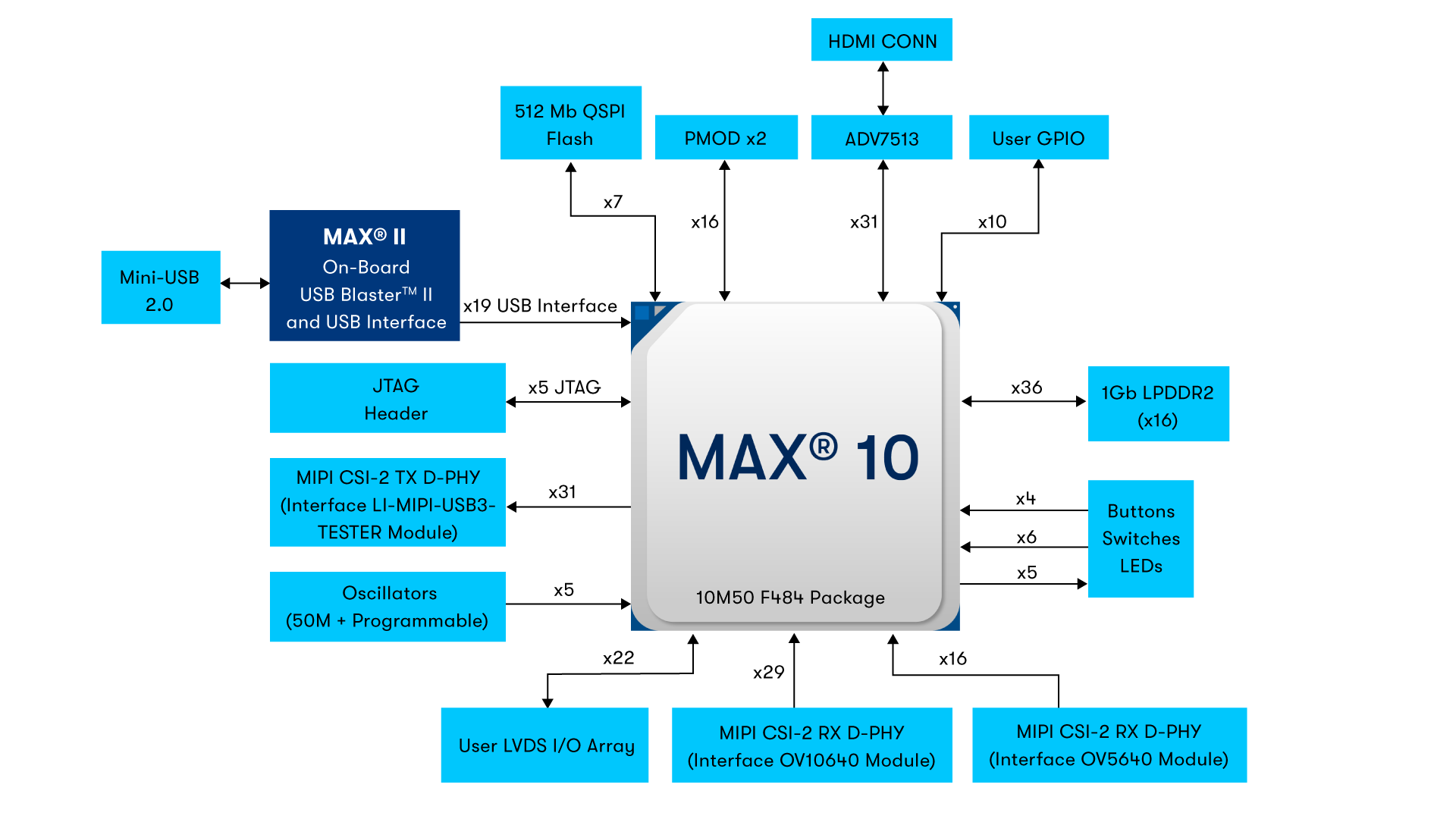
MAX 10 FPGA system architecture and resource diagram
Four PLLs provide flexible clock management with frequency synthesis, phase shifting, and spread-spectrum clocking. The integrated 12-bit ADC supports up to 18 analog input channels at 1 MSPS, ideal for sensor interfacing and power monitoring without external ADC ICs. Internal flash memory stores up to two configuration images, enabling instant-on operation and secure remote field updates. The user flash memory (UFM) offers non-volatile storage for calibration data, encryption keys, or application parameters.
5. Typical Applications & Circuit Design
The 10M16SAU169I7G is widely used in industrial, communications, and embedded applications where non-volatile, instant-on FPGA functionality is critical. Common use cases include:
- Industrial Motor Control: PWM generation, encoder interfaces, and real-time control loops using embedded multipliers
- Sensor Hub / IoT Gateway: Integrated ADC for direct sensor acquisition, I/O bridging, and protocol conversion
- Communication Infrastructure: SPI/I2C/UART protocol bridges, LED matrix drivers, and display controllers
- Power Management: Sequencing control, voltage monitoring via the built-in ADC, and system health reporting
- Prototyping & Education: Low-cost FPGA development with the MAX 10 evaluation boards available at wwdparts
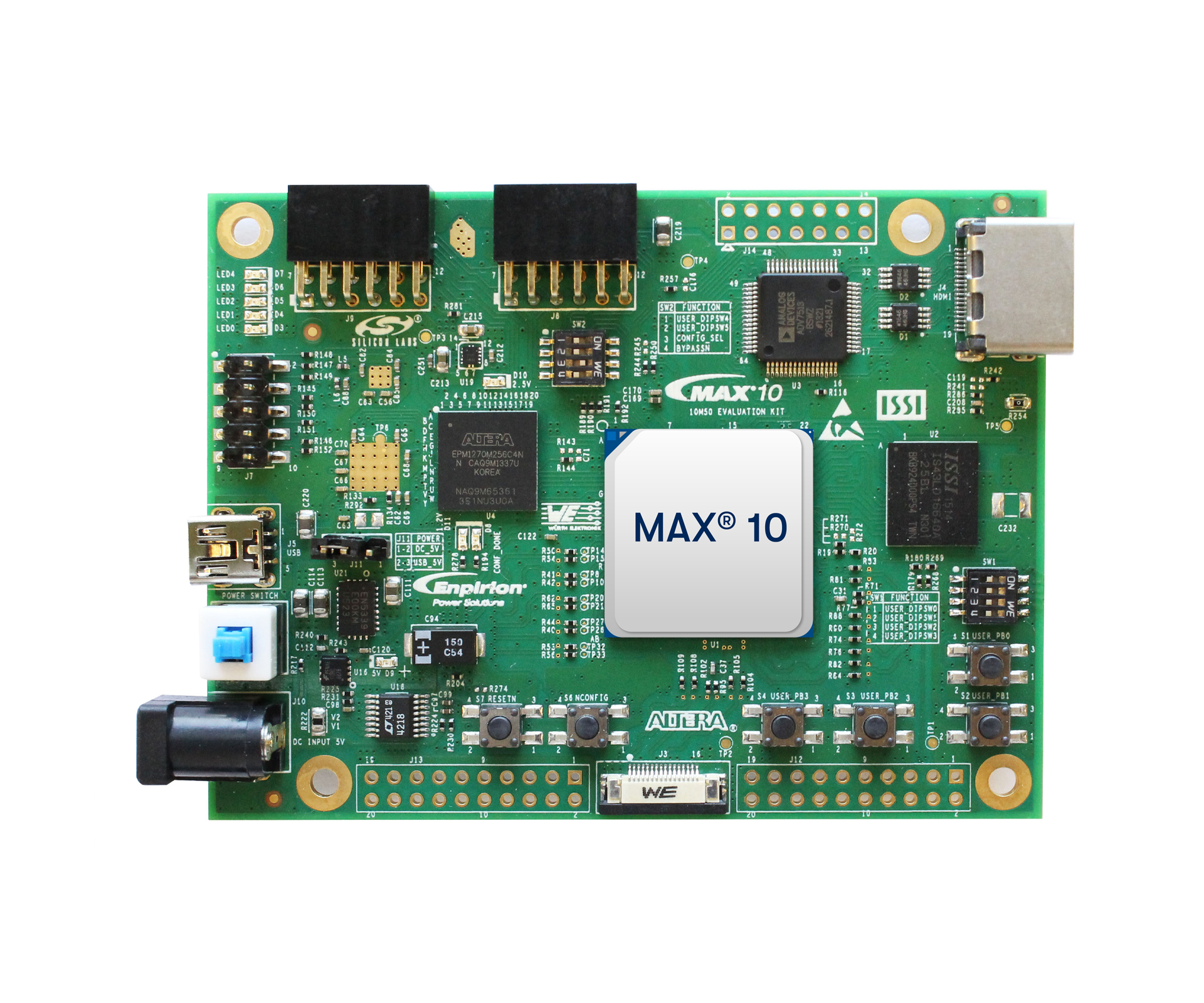
MAX 10 FPGA evaluation board for rapid prototyping
The instant-on configuration eliminates boot delays, which is essential for safety-critical and real-time systems. Dual-image configuration supports fail-safe remote updates - if a new configuration image fails, the device automatically reverts to the golden image. For design resources and reference schematics, visit the wwdparts technical blog.
Video Tutorial: Getting Started with MAX 10 FPGA
6. Ordering & Availability
The 10M16SAU169I7G is available from authorized distributors worldwide. When ordering, verify the full part number to ensure the correct temperature grade (I = Industrial, C = Commercial) and speed grade (7). Key ordering details:
| Detail | Value |
|---|---|
| Manufacturer Part Number | 10M16SAU169I7G |
| Manufacturer | Intel (Altera) |
| Category | FPGAs - Field Programmable Gate Arrays |
| Package | 169-UBGA |
| Temperature Grade | Industrial (-40 °C to +100 °C) |
| Speed Grade | 7 |
| RoHS Status | Compliant (Lead-Free) |
| Lifecycle Status | Active |
For competitive pricing and guaranteed authentic stock, check the wwdparts.com inventory or contact our sales team for volume quotes and lead time estimates.
Frequently Asked Questions (FAQ)
What is the 10M16SAU169I7G?
The 10M16SAU169I7G is an Intel MAX 10 FPGA featuring 16,000 logic elements, 549 Kb embedded RAM, a 12-bit ADC, and 130 user I/O pins in a compact 169-UBGA package. It operates over the industrial temperature range of -40 °C to +100 °C.
What package does the 10M16SAU169I7G use?
It uses a 169-ball Ultra Fine-Line BGA (UBGA) package measuring 11 mm x 11 mm with a 0.8 mm ball pitch. This surface-mount package is designed for compact, space-constrained PCB layouts.
Does the 10M16SAU169I7G have an integrated ADC?
Yes, it includes a 12-bit analog-to-digital converter capable of up to 1 MSPS sampling rate with up to 18 analog input channels. This enables direct sensor interfacing without external ADC components.
What is the operating temperature range?
The 10M16SAU169I7G is rated for the industrial temperature range of -40 °C to +100 °C (junction temperature), suitable for harsh-environment applications in factory automation, outdoor equipment, and transportation systems.
Does the 10M16SAU169I7G require external configuration memory?
No. MAX 10 FPGAs feature internal flash-based configuration storage, eliminating the need for external configuration PROMs or flash chips. The device supports dual configuration images for fail-safe remote updates and powers up instantly.
What development tools are needed for the 10M16SAU169I7G?
Intel Quartus Prime Lite Edition (free) fully supports the MAX 10 family. Design entry options include Verilog HDL, VHDL, and schematic capture. Programming is done via a USB Blaster or USB Blaster II through the JTAG interface.


