
1. 10M08SAE144C8G Overview
The 10M08SAE144C8G is a non-volatile FPGA from the Intel (Altera) MAX 10 family, built on 55 nm flash technology. It delivers 8,000 logic elements, an integrated 12-bit ADC, and dual configuration flash in a compact 144-pin EQFP package — all without requiring an external configuration device. Its "instant-on" capability and single-chip architecture make it a compelling choice for system management, I/O expansion, industrial control, and cost-sensitive embedded designs where both FPGA flexibility and rapid boot time are essential.
Supported by the free Quartus Prime Lite Edition, the 10M08SAE144C8G lowers the barrier to entry for both prototyping and volume production. The MAX 10 family also integrates user flash memory (UFM) for on-chip data storage, eliminating the need for external serial flash in many applications.
2. Key Specifications & Parameters
| Parameter | Value |
|---|---|
| Manufacturer | Intel (Altera) |
| Family | MAX 10 FPGA |
| Part Number | 10M08SAE144C8G |
| Logic Elements (LEs) | 8,000 |
| M9K Memory Blocks | 378 Kb (42 blocks) |
| Total RAM Bits | 387,072 |
| User Flash Memory (UFM) | 32 KB typical (up to 172 KB) |
| Embedded Multipliers (18x18) | 24 |
| PLLs | 2 |
| Max User I/O Pins | 101 |
| ADC | 1-channel, 12-bit, 1 MSPS |
| Package | 144-EQFP (22 mm x 22 mm) |
| Process Technology | 55 nm |
| Core Voltage (VCCINT) | 1.2 V |
| I/O Voltage | 3.3 V (multi-standard support) |
| Speed Grade | C8 (Commercial, 0 C to 85 C) |
| Configuration | Internal dual-image flash, JTAG |
| Quartus Support | Quartus Prime Lite (free) |
3. Block Diagram & Architecture
The Intel MAX 10 architecture integrates logic array blocks (LABs), M9K embedded memory, DSP blocks with 18x18 multipliers, analog-to-digital converters, user flash memory, and dual configuration flash into a single monolithic die. Each LAB contains 16 logic elements, and the routing fabric supports high-utilization designs up to 300 MHz+ in typical applications.

Figure 1: Intel MAX 10 FPGA device architecture block diagram.
4. Pinout & Package Information
The 10M08SAE144C8G ships in a 144-pin Enhanced Quad Flat Package (EQFP) measuring 22 mm x 22 mm with 0.5 mm pin pitch and an exposed thermal pad. Of the 144 pins, 101 are available as user I/O, organized into multiple I/O banks supporting LVTTL, LVCMOS, SSTL, and HSTL standards. The exposed pad should be soldered to the ground plane for optimal thermal and electrical performance.

Figure 2: 10M08SAE144C8G 144-EQFP package footprint.
5. Applications & Evaluation Kit
The 10M08SAE144C8G excels in a wide range of embedded applications:
- System management & board management controllers (BMC) — instant-on boot enables watchdog and supervisory functions
- I/O expansion & protocol bridging — SPI, I2C, UART, and custom interfaces
- Industrial control & motor drive — integrated ADC simplifies sensor acquisition
- Automotive infotainment & ADAS preprocessing
- Consumer electronics & IoT edge nodes
Intel offers the MAX 10 FPGA 10M08 Evaluation Kit (EK-10M08E144) featuring Arduino-compatible headers, on-board USB-Blaster for JTAG programming, push buttons, LEDs, and an analog input front-end connected to the on-chip ADC.
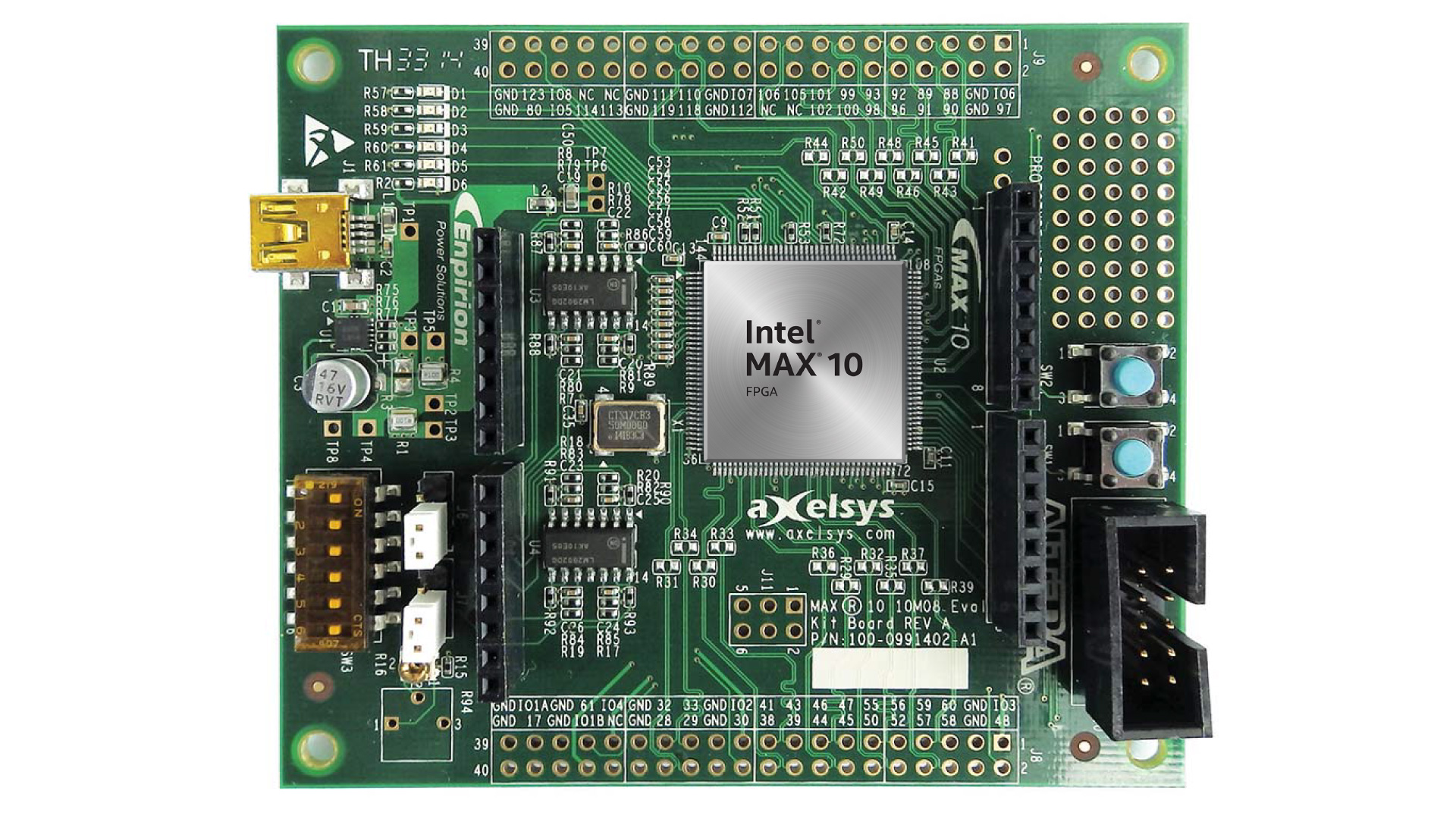
Figure 3: MAX 10 FPGA 10M08 Evaluation Kit.
Getting Started: Video Tutorial
Watch this tutorial to get started with Intel MAX 10 FPGA development and Quartus Prime:
6. Frequently Asked Questions
What is the 10M08SAE144C8G?
The 10M08SAE144C8G is a non-volatile FPGA from Intel's MAX 10 family. It provides 8,000 logic elements, 378 Kb of M9K embedded memory, an integrated 12-bit ADC, and dual configuration flash in a 144-pin EQFP package. Built on 55 nm flash technology, it boots instantly without an external configuration device.
Does the 10M08SAE144C8G require an external configuration memory?
No. The MAX 10 family integrates dual configuration flash on-die, so the 10M08SAE144C8G configures itself at power-up in under 10 milliseconds. This instant-on feature eliminates the need for external serial flash devices typically required by other FPGA families.
What software do I need to program the 10M08SAE144C8G?
You can use Quartus Prime Lite Edition, which is free to download from Intel/Altera. It supports design entry in Verilog, VHDL, or schematic capture, and programs the device via JTAG using a USB-Blaster or USB-Blaster II cable.
What is the operating temperature range of the 10M08SAE144C8G?
The C8G suffix indicates the commercial temperature grade, which operates from 0 C to 85 C. Intel also offers industrial (-I7G, -40 C to 100 C) and automotive (-A7G) variants of the MAX 10 family for extended temperature applications.
Can the 10M08SAE144C8G be used for analog signal acquisition?
Yes. The device integrates a 12-bit successive-approximation ADC capable of 1 MSPS. It supports up to 18 analog input channels (depending on the package variant) and includes a built-in temperature sensor. The ADC IP is configured through the Quartus Prime IP Catalog.
What is the difference between 10M08SAE144C8G and 10M08SAE144I7G?
Both share the same die and 144-EQFP package. The C8G is commercial grade (0-85 C, speed grade 8), while the I7G is industrial grade (-40-100 C, speed grade 7). The industrial variant is tested and guaranteed over a wider temperature range, making it suitable for harsh-environment applications.
Related Components at wwdparts.com
- 10M04SCE144C8G — MAX 10 FPGA, 4,000 LEs, 144-EQFP, ideal for lower-density designs
- 10M16SAE144C8G — MAX 10 FPGA, 16,000 LEs, 144-EQFP, pin-compatible upgrade path
- 5M160ZE64C5N — MAX V CPLD for simpler glue-logic and I/O expansion tasks


