
The 10M16SAU169I7G is a non-volatile FPGA from the Intel (Altera) MAX 10 family. Built on 55nm technology, this device integrates 16,000 logic elements, embedded flash memory, an analog-to-digital converter, and PLLs into a compact 169-pin UBGA package. It is designed for cost-sensitive, low-power embedded applications where instant-on capability and single-chip integration are critical.
Table of Contents
- Overview & Key Features
- Technical Specifications
- Block Diagram & Architecture
- Pinout & Package Information
- Application Circuit & Design Resources
- Frequently Asked Questions
Overview & Key Features
The 10M16SAU169I7G belongs to the Intel MAX 10 FPGA family, which revolutionizes non-volatile integration by combining advanced processing capabilities with internal configuration storage. Unlike traditional FPGAs that require external configuration memory, MAX 10 devices store their configuration in on-chip flash, enabling instant-on operation within milliseconds of power-up.
Key highlights of the 10M16SAU169I7G include:
- 16,000 Logic Elements (LEs) — sufficient for mid-complexity digital designs
- Dual-boot support — two configuration images in internal flash for safe remote updates
- Integrated ADC — on-chip analog-to-digital converter eliminates external ADC components
- User flash memory — non-volatile storage for application data and coefficients
- Industrial temperature range — rated for –40 °C to +100 °C operation
- Low power — 1.2 V core voltage with advanced power management
This device is ideal for industrial control systems, motor drives, sensor hubs, and IoT edge processing where a single-chip programmable solution reduces board space and BOM cost.
Technical Specifications
| Parameter | Value |
|---|---|
| Part Number | 10M16SAU169I7G |
| Manufacturer | Intel (Altera) |
| Family | MAX 10 (10M16) |
| Logic Elements (LEs) | 16,000 |
| Logic Array Blocks (LABs) | 1,000 |
| Embedded Memory (M9K blocks) | 549 Kb (62 M9K blocks) |
| User Flash Memory | 2,876 Kb |
| 18×18 Multipliers | 45 |
| PLLs | 4 |
| Maximum User I/O Pins | 130 |
| LVDS Pairs | Up to 22 |
| Analog-to-Digital Converter | 1 ADC (up to 18 channels, 12-bit) |
| Core Voltage | 1.2 V |
| I/O Voltage | 3.0 V / 3.3 V (LVTTL/LVCMOS) |
| Speed Grade | 7 (slowest) |
| Temperature Range | –40 °C to +100 °C (Industrial) |
| Package | 169-UBGA (11 × 11 mm) |
| Process Technology | 55 nm |
| Configuration | Internal flash (instant-on, dual-image boot) |
| External Memory Interface | DDR2, DDR3, LPDDR2, SRAM |
| I/O Standards | LVTTL, LVCMOS, PCI, SSTL, HSTL, LVDS |
| Lead-Free / RoHS | Yes (Green / RoHS compliant) |
Block Diagram & Architecture
The MAX 10 architecture integrates programmable logic, embedded memory, DSP multiplier blocks, PLLs, and a unique analog-to-digital converter on a single die. The device floorplan places I/O banks around the perimeter, with the logic array, M9K memory blocks, and embedded multipliers in the core. The on-chip flash memory block handles both FPGA configuration and user data storage.
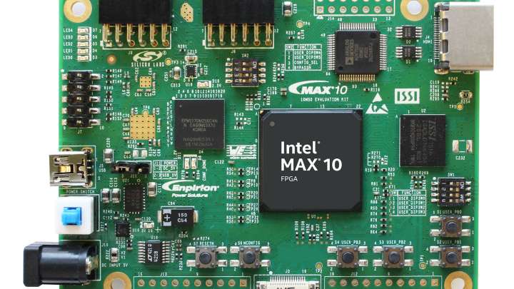
Figure 1: Intel MAX 10 FPGA architecture overview showing key functional blocks.
The logic array is built from Logic Array Blocks (LABs), each containing 16 logic elements. Each LE includes a 4-input look-up table (LUT), a programmable register, and carry chain logic. The M9K embedded memory blocks provide 9 Kb each and can be configured as single-port RAM, dual-port RAM, ROM, or FIFO buffers.
Pinout & Package Information
The 10M16SAU169I7G uses a 169-ball UBGA (Ultra Fine-pitch Ball Grid Array) package with an 11 × 11 mm body size and 0.8 mm ball pitch. The compact footprint makes it suitable for space-constrained designs in industrial and IoT applications.

Figure 2: 10M16SAU169I7G in 169-UBGA package.
The U169 package provides 130 user I/O pins organized into multiple I/O banks, supporting a variety of I/O standards from 1.2 V to 3.3 V. Dedicated pins include JTAG configuration, clock inputs, and ADC analog input channels. Designers should refer to the official Intel pin-out files for detailed ball-map assignments.
Application Circuit & Design Resources
The MAX 10 FPGA family is widely used in evaluation kits and reference designs. Intel provides development kits centered around MAX 10 devices, featuring on-board USB-Blaster programming, Arduino-compatible headers, and analog front-end circuits for ADC evaluation.
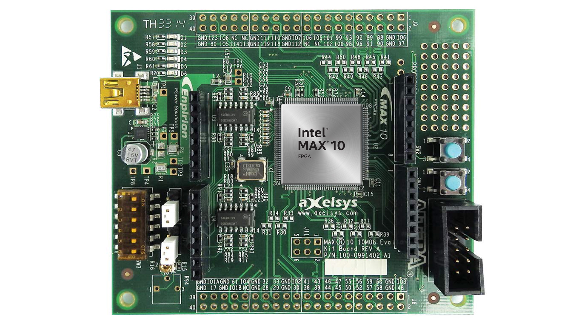
Figure 3: MAX 10 FPGA Evaluation Kit board for rapid prototyping and development.
Typical application circuits with the 10M16SAU169I7G include:
- Motor control — PWM generation, encoder interface, and PID loops implemented in FPGA logic
- Sensor aggregation — using the built-in ADC and I/O to interface multiple analog and digital sensors
- Protocol bridging — converting between industrial protocols (SPI, I²C, UART, Modbus) with low latency
- Video/display processing — driving HDMI outputs using LVDS pairs with embedded frame buffers
Design tools include Quartus Prime Lite Edition (free), which supports full synthesis, place-and-route, timing analysis, and JTAG programming for all MAX 10 devices. Browse more Intel Altera FPGA components for your design needs.
Video Tutorial: Getting Started with MAX 10 FPGA
Frequently Asked Questions
What is the 10M16SAU169I7G?
The 10M16SAU169I7G is an Intel (Altera) MAX 10 FPGA with 16,000 logic elements in a 169-UBGA package. It features internal configuration flash memory, an integrated 12-bit ADC, 549 Kb of embedded RAM, 45 multipliers, and 4 PLLs, making it a complete system-on-chip solution for embedded applications.
What is the operating temperature range of the 10M16SAU169I7G?
The "I" suffix in the part number indicates Industrial temperature grade, supporting operation from –40 °C to +100 °C. This makes it suitable for harsh environments including factory automation, outdoor equipment, and automotive-adjacent systems.
Does the 10M16SAU169I7G require an external configuration memory?
No. MAX 10 FPGAs store their configuration in on-chip flash memory, eliminating the need for external serial configuration devices (like EPCS/EPCQ). The device supports dual-image boot, allowing safe remote field updates with automatic fallback to a known-good image.
What software is used to program the 10M16SAU169I7G?
Intel's Quartus Prime Lite Edition is the free EDA tool that supports MAX 10 FPGA design. It provides schematic capture, Verilog/VHDL synthesis, simulation (via ModelSim-Intel), timing analysis, and JTAG/In-System programming. The Lite edition has no license fee and supports all MAX 10 device variants.
How many I/O pins are available on the 10M16SAU169I7G?
The U169 package variant provides 130 user I/O pins. These support multiple I/O standards including 3.3 V LVTTL, 2.5 V / 1.8 V / 1.5 V / 1.2 V LVCMOS, SSTL, HSTL, and up to 22 LVDS differential pairs for high-speed interfaces.
What are common alternatives to the 10M16SAU169I7G?
Common alternatives within the MAX 10 family include the 10M08SAU169I7G (8K LEs, same package), 10M16SAE144I7G (16K LEs, 144-EQFP package), and the 10M50DAF484I7G (50K LEs for higher density). For cross-family alternatives, consider the Lattice MachXO3 or Microchip PolarFire SoC families.


