
10M16SAU169I7G: Datasheet, Pinout, Block Diagram & Application Guide | Altera MAX 10 FPGA
The 10M16SAU169I7G is a non-volatile, single-chip FPGA from Altera’s (now Intel) MAX 10 family, fabricated on TSMC’s 55 nm embedded flash process. It integrates 16,000 logic elements, 549 Kbit of M9K embedded SRAM, 45 hardware 18×18-bit multipliers, dual on-die configuration flash images, a 12-bit 1 MSPS SAR ADC with dedicated analog channels, and 4 PLLs — all within a compact 169-pin UBGA package measuring 11×11 mm. Rated for the industrial temperature range (−40 °C to +100 °C) at speed grade 7, the 10M16SAU169I7G eliminates external configuration memory, reducing BOM cost and board area for harsh-environment industrial control, automotive peripherals, IoT edge, and portable instrumentation applications.
Overview and Part Number Decoding
The 10M16SAU169I7G belongs to the Altera MAX 10 product line — the industry’s first single-chip, non-volatile FPGA family. Unlike SRAM-based FPGAs such as Xilinx Spartan-7 or Intel Cyclone V that require external SPI flash for configuration bitstream storage, MAX 10 devices store up to two complete configuration images in on-die flash memory. This architecture enables instant-on operation within milliseconds of power-up and supports fail-safe remote field updates via the Remote System Upgrade (RSU) IP core — without any external EPCQ or SPI NOR flash on the BOM.
With 16,000 logic elements, the 10M16SAU169I7G is the mid-density workhorse of the MAX 10 lineup, providing double the logic capacity of the 10M08 variants while maintaining a remarkably small 11×11 mm BGA footprint. The “I7” designation marks this as the industrial-grade variant, qualified for continuous operation from −40 °C to +100 °C — essential for factory-floor, outdoor, and transportation applications where commercial-grade devices cannot meet reliability requirements.
The part number encodes the following attributes:
- 10M16 — MAX 10 family, 16,000 logic elements
- SA — Single-supply, Analog variant (internal 1.2 V regulator, integrated 12-bit ADC)
- U169 — 169-pin Ultra-Fine-Pitch Ball Grid Array (UBGA), 11×11 mm, 0.8 mm ball pitch
- I7 — Industrial temperature range (−40 °C to +100 °C), speed grade 7
- G — Green / RoHS / Pb-free compliant
The “SA” designation indicates this is the analog-enabled variant that includes a dual 12-bit, 1 MSPS SAR ADC with dedicated external analog input channels and an internal temperature sensor — distinguishing it from the “SC” (Compact) variants that lack the integrated ADC. The device is fully supported by Intel Quartus Prime Lite Edition, which is free to download and requires no license file. For current stock and pricing, check 10M16SAU169I7G availability on WWDParts.
Specifications and Parameter Table
| Parameter | Value |
|---|---|
| Manufacturer | Altera (Intel) |
| Product Family | MAX 10 |
| Part Number | 10M16SAU169I7G |
| Logic Elements (LEs) | 16,000 |
| Logic Array Blocks (LABs) | 1,000 (16 LEs per LAB) |
| M9K Embedded Memory Blocks | 61 |
| Total Embedded SRAM | 549 Kbit |
| 18×18 Embedded Multipliers | 45 |
| Phase-Locked Loops (PLLs) | 4 (4 output counters each) |
| Integrated ADC | Dual 12-bit, 1 MSPS SAR ADC (dedicated analog channels + internal temperature sensor) |
| User Flash Memory (UFM) | 736 Kbit |
| Configuration Flash Memory | Dual-image internal flash (instant-on, <10 ms boot) |
| User I/O Pins (U169 package) | 130 |
| I/O Banks | 8 |
| Maximum LVDS Differential Pairs | 22 |
| I/O Standards Supported | 3.3 V / 2.5 V / 1.8 V / 1.5 V LVTTL/LVCMOS, LVDS, SSTL, HSTL, PCI |
| Maximum Fabric Frequency | ~400 MHz (register-to-register, speed grade 7) |
| M9K Maximum Speed | ~260 MHz |
| Core Voltage (VCC) | 1.2 V (internally regulated from 3.3 V) |
| External Supply (VCCA / VCCIO) | 3.3 V single rail (2.85–3.465 V) |
| Process Technology | 55 nm (TSMC embedded NOR flash) |
| Package | 169-UBGA (11 × 11 mm body, 0.8 mm ball pitch) |
| Operating Temperature | −40 °C to +100 °C (Industrial) |
| Speed Grade | 7 |
| DDR Memory Interface | DDR2, DDR3, LPDDR2, SRAM |
| Bitstream Security | Yes (AES-128 encryption) |
| RoHS Compliant | Yes (Pb-free) |
| Lifecycle Status | Active (2026) |
Looking for 10M16SAU169I7G Inventory?
Check our real-time stock levels, pricing, and volume discounts for global distribution.
Check 10M16SAU169I7G StockArchitecture and Block Diagram
The MAX 10 FPGA architecture is organized around a fabric of configurable logic, embedded memory, and DSP resources interconnected by a hierarchical routing network with 20 global clock networks. The 10M16SAU169I7G integrates six core building blocks:
- 16,000 Logic Elements (LEs): Each LE contains a 4-input look-up table (LUT), a programmable register with synchronous load and asynchronous clear, carry chain logic, and register feedback. LEs are grouped into 1,000 Logic Array Blocks (LABs) of 16 LEs each, with dedicated local interconnect enabling fast intra-LAB routing at minimal skew.
- 61 M9K Memory Blocks (549 Kbit): Each 9,216-bit block (including parity) is configurable as single-port RAM, simple dual-port RAM, true dual-port RAM, ROM, or FIFO buffer. Supports data widths from ×1 to ×36 with byte-enable control, operating at up to 260 MHz at speed grade 7.
- 45 Embedded 18×18-bit Multipliers: Dedicated DSP blocks for arithmetic operations. Each block operates as one 18×18-bit multiplier or splits into two independent 9×9-bit multipliers — suitable for FIR filters, PID control loops, motor drive algorithms, and fixed-point arithmetic pipelines.
- 4 PLLs: On-chip phase-locked loops provide clock synthesis, multiplication (up to ×512), division, and dynamic phase shifting. Input frequency range spans 5 MHz to 472.5 MHz with up to 4 independent output clocks per PLL, each with lock detect and dynamic reconfiguration.
- Dual Configuration Flash + 736 Kbit UFM: Two on-die configuration images enable fail-safe remote updates via the RSU IP core. The User Flash Memory stores calibration constants, serial numbers, or firmware data non-volatilely, accessible at runtime through the UFM IP core or Avalon-MM interface.
- Dual 12-bit ADC: The “SA” variant includes two 12-bit, 1 MSPS successive approximation register (SAR) ADCs with dedicated analog input channels. An internal temperature sensor is also accessible. The ADC supports single-ended input ranges of 0–2.5 V (with external reference) and is controlled via a dedicated Modular ADC IP core in Platform Designer.
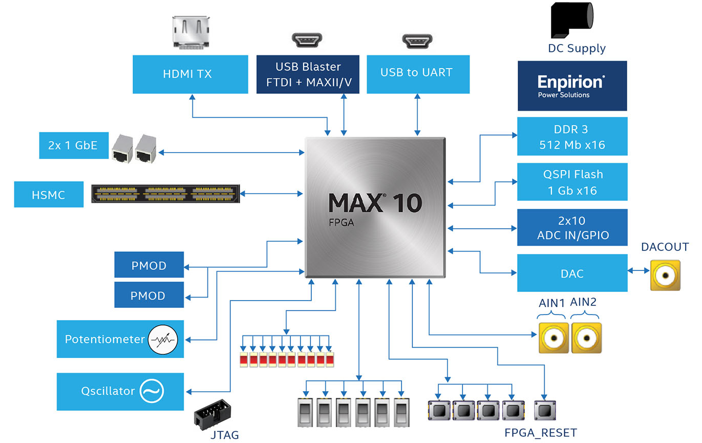
Figure 1: Altera MAX 10 FPGA development kit block diagram — configurable logic fabric, embedded memory, PLLs, DSP blocks, integrated ADC, user flash, and I/O interfaces. The 10M16SAU169I7G implements this architecture with 16K LEs, 61 M9K blocks, 45 multipliers, and dual 12-bit ADCs.
Pinout, Package, and PCB Layout
The 10M16SAU169I7G is housed in a 169-pin UBGA (Ultra-Fine-Pitch Ball Grid Array) with a body size of 11 mm × 11 mm, 0.8 mm ball pitch in a 13×13 ball array. The package provides 130 user I/O pins organized across 8 I/O banks, each with an independent VCCIO supply rail for mixed-voltage interfacing. The compact BGA footprint makes it ideal for space-constrained designs where a 144-EQFP is too large.
Key pinout and layout considerations:
- VCCIO Banks: Each I/O bank supports independent VCCIO. For the “SA” single-supply variant, all VCCIO pins are typically tied to 3.3 V. Mixed-voltage designs can set individual banks to 2.5 V, 1.8 V, or 1.5 V for direct interfacing to external ICs.
- Analog Input Pins: The ADC analog input pins are shared with digital I/O on dedicated banks. When the ADC is enabled, these pins are dedicated analog inputs with a 0–2.5 V input range. Route analog traces away from digital switching signals and provide a low-noise VREFP/VREFN pair from a precision reference.
- JTAG Pins (TCK, TDI, TDO, TMS): Dedicated configuration and boundary-scan pins. Apply 10 kΩ pull-up resistors on TDI and TMS, even when JTAG is unused in production — these pins must not float.
- MSEL[0]: Configuration mode select. Tie to GND for internal configuration mode (standard for MAX 10 instant-on operation).
- Power / Ground: All VCC and GND balls must be connected. Place 100 nF MLCC decoupling capacitors on every power ball, plus a 10 µF bulk capacitor per supply rail near the device.
- BGA Routing: The 0.8 mm ball pitch requires careful PCB routing. Use 4-layer minimum stackup with 75 µm (3-mil) trace/space on signal layers. Place via-in-pad with cap plating for inner-row ball breakout.
- Industrial Temperature Considerations: For −40 °C to +100 °C operation, ensure thermal relief pads on all power balls. Perform thermal simulation to verify junction temperature stays below 100 °C at maximum ambient, accounting for the internal regulator power dissipation.
Figure 2: 10M16SAU169I7G in 169-UBGA package — 11 × 11 mm body, 13×13 ball array, 0.8 mm pitch. Compact BGA footprint ideal for space-constrained industrial and IoT designs.
Application Circuits and Design Guidelines
The 10M16SAU169I7G targets systems requiring instant-on, non-volatile programmable logic with integrated analog-to-digital conversion, industrial-grade temperature tolerance, and minimal external component count. With 16,000 LEs and 45 multipliers, it offers sufficient resources for medium-complexity digital signal processing, protocol bridging, and mixed-signal system control. Typical application domains include:
- Industrial Automation: Motor drive encoder interfaces, PLC I/O expansion modules, sensor aggregation hubs, and protocol bridging (SPI ↔ UART, I2C ↔ parallel bus). The instant-on capability ensures deterministic control outputs within milliseconds of power-up, while the integrated ADC reads temperature, current, and voltage sensors directly without external converter ICs. The industrial temperature rating (−40 °C to +100 °C) is essential for factory-floor deployment near heat sources.
- Communications Equipment: Small-cell baseband glue logic, Ethernet MAC-to-PHY bridging, CPRI/OBSAI framing, and multi-protocol serial conversion. The 45 embedded multipliers handle DSP pre-processing in the datapath, and the ADC monitors RF power levels and supply rails.
- Board Management Controllers: Voltage rail power sequencing, system health monitoring (temperature, current), fan speed control, and watchdog supervision. The dual-image flash enables safe firmware updates in the field, and the on-chip ADC samples all critical supply voltages without requiring external ADC ICs.
- Transportation & Outdoor IoT: Smart sensor hubs for rail and automotive peripheral systems, traffic control modules, and environmental monitoring stations. The extended temperature range ensures reliable operation across extreme seasonal and geographic conditions without derating.
Power Supply Design: The “SA” single-supply variant requires only a single 3.3 V rail (2.85–3.465 V). The internal 1.2 V core regulator draws approximately 80–300 mA depending on logic utilization and clock frequency. The ADC block requires a separate VREFP reference (typically 2.5 V from an external precision reference such as the REF3025 or ADR3425) for accurate analog conversions.
PCB Layout Best Practices:
- Use a 4-layer minimum stackup (signal–ground–power–signal) with dedicated power and ground planes
- For 0.8 mm BGA breakout, use via-in-pad with cap plating on inner-row balls; route escape channels on inner layers
- Route clock signals on inner layers with 50 Ω controlled impedance; use 100 Ω differential for LVDS pairs
- Keep PLL input clock trace lengths under 50 mm with length-matched output clock routing
- Provide a 10-pin JTAG header (2×5, 2.54 mm pitch) with trace lengths under 150 mm
- Tie MSEL[0] to GND for internal configuration; the device boots in under 10 ms from power-up
- Isolate ADC analog inputs with a guard ring; route analog traces on a separate layer from high-speed digital signals
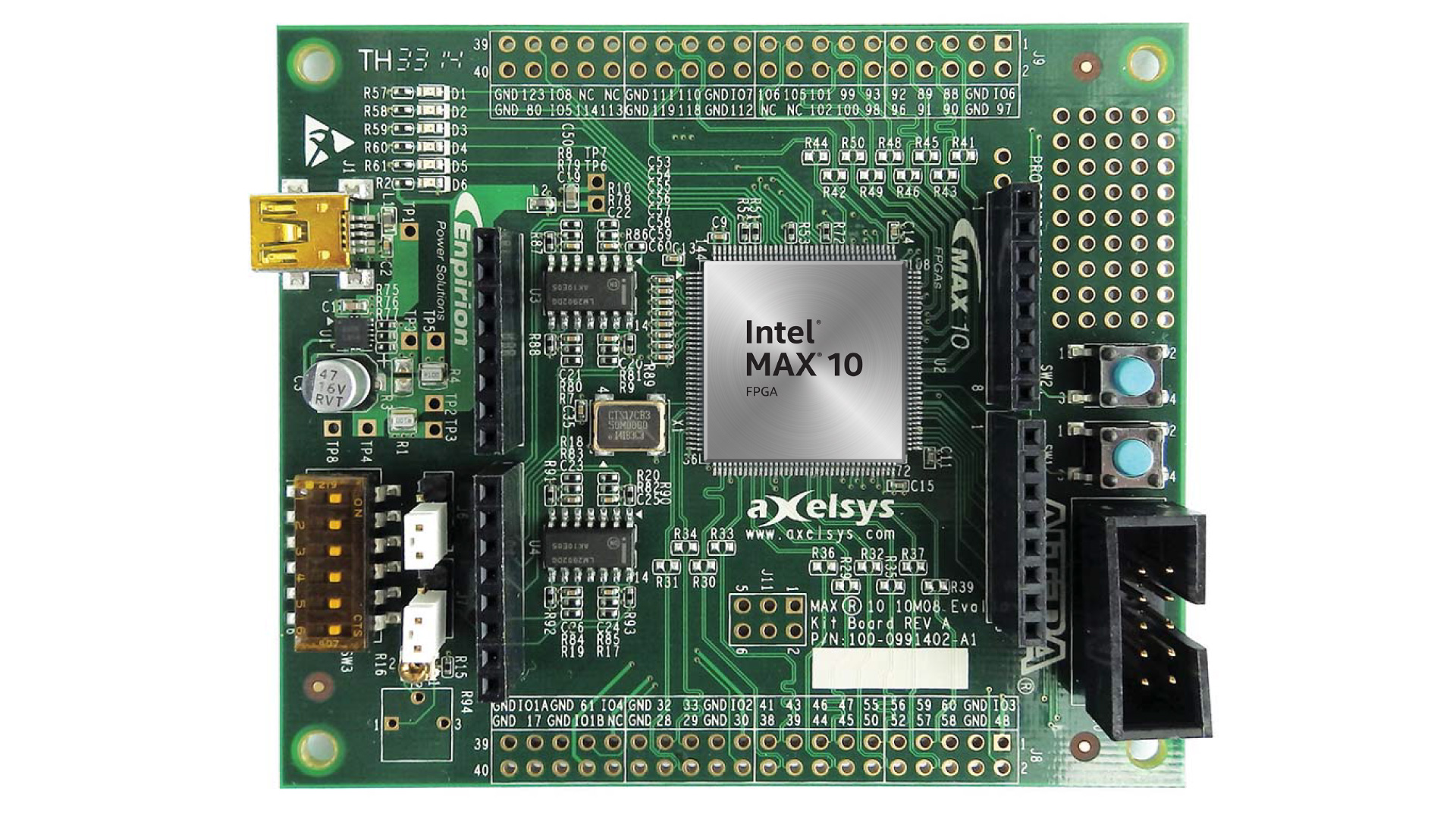
Figure 3: MAX 10 FPGA evaluation board — a typical application platform showing power supply section, JTAG programming, user I/O headers, and peripheral expansion for prototyping with MAX 10 devices including the 10M16SAU169I7G.
Equivalents, Cross-Reference, and Lifecycle
The 10M16SAU169I7G carries an Active lifecycle status as of 2026 and is broadly stocked by major distributors including Digi-Key, Mouser, Arrow, and LCSC.
Pin-compatible alternatives within the MAX 10 family:
- 10M16SAU169C8G — Commercial temperature variant (0 °C to +85 °C) at speed grade 8. Pin-compatible drop-in with faster timing but narrower temperature range.
- 10M16SCU169I7G — The “SC” Compact variant in the same 169-UBGA package at industrial temperature. Pin-compatible drop-in that omits the ADC.
- 10M08SAU169I7G — Same package, ADC, and industrial temperature rating, reduced to 8,000 LEs with 378 Kbit embedded RAM. Pin-compatible cost-down option.
Cross-vendor alternatives:
- Lattice MachXO3LF-9400 (LCMXO3LF-9400C-6BG256I): Comparable logic density (~9,400 LUTs) with integrated flash and industrial temperature. Requires Lattice Diamond; pinout is not compatible.
- Microchip PolarFire MPF100T: Higher-density, low-power flash FPGA for designs outgrowing MAX 10 capacity.
Unit pricing for the 10M16SAU169I7G typically falls in the $15–$30 USD range depending on quantity. To check real-time stock, pricing, or request a quote, upload your BOM to WWDParts for fast processing.
Video: Getting Started with Altera MAX 10 FPGA Development
Video: Programming the Terasic DE10-Lite board (Altera MAX 10 FPGA) with Quartus — applicable to 10M16SAU169I7G development workflow.
Related technical guides on WWDParts:
- 10M16SAU169C8G Datasheet, Specs & Pinout | Intel MAX 10 FPGA
- 10M08SAE144C8G Datasheet, Pinout, Block Diagram & Application Guide
- 10M04SCE144C8G Datasheet, Pinout, Block Diagram & Application Guide
Frequently Asked Questions (FAQ)
What is the 10M16SAU169I7G and what makes it unique?
The 10M16SAU169I7G is an industrial-grade, non-volatile FPGA from Altera’s MAX 10 family with 16,000 logic elements, 549 Kbit of M9K SRAM, 45 embedded multipliers, and a dual 12-bit ADC — all in a compact 169-UBGA package (11×11 mm). Its unique value lies in integrating configuration flash on-die for instant-on boot in under 10 ms with no external configuration memory required, combined with an industrial temperature rating of −40 °C to +100 °C.
Does the 10M16SAU169I7G require an external configuration memory?
No. MAX 10 FPGAs store up to two complete configuration bitstream images in on-die flash memory, eliminating the need for external EEPROM or SPI NOR flash. This enables instant-on operation (<10 ms from power-up to active I/O) and supports fail-safe Remote System Upgrade (RSU) — if a new image fails, the device automatically reverts to the known-good backup image.
What design software supports the 10M16SAU169I7G?
Intel Quartus Prime Lite Edition (free, no license required) fully supports all MAX 10 devices for design entry, synthesis, place-and-route, and timing analysis. A USB-Blaster or USB-Blaster II JTAG cable is needed for programming and SignalTap debugging. The Quartus package includes Platform Designer (formerly Qsys) for system integration, the Modular ADC IP core for configuring the on-chip ADC, and ModelSim-Intel FPGA Starter Edition for RTL simulation.
What is the difference between 10M16SAU169I7G and 10M16SAU169C8G?
Both share the same 16,000 LE logic fabric, 549 Kbit SRAM, 45 multipliers, ADC, and 169-UBGA package with identical pinouts. The key differences are temperature range and speed grade: the I7G variant operates from −40 °C to +100 °C (industrial) at speed grade 7, while the C8G variant operates from 0 °C to +85 °C (commercial) at speed grade 8 with slightly faster timing. Choose the I7G for harsh-environment deployments; choose C8G for cost-sensitive consumer applications.
Can I use the integrated ADC for precision measurement?
The dual 12-bit ADC operates at up to 1 MSPS per channel and is well suited for monitoring supply voltages, temperature sensors, and low-frequency analog signals such as current shunts and potentiometer inputs. For high-precision measurement applications requiring better INL/DNL performance (e.g., <1 LSB), consider using an external precision ADC such as the ADS1115 or AD7689 alongside the FPGA. The integrated ADC is controlled through the Modular ADC IP core in Quartus Prime Platform Designer.
Where can I buy the 10M16SAU169I7G and what is the typical pricing?
The 10M16SAU169I7G is available from WWDParts, an authorized semiconductor distributor offering competitive pricing, datasheets, and fast global shipping. Unit pricing typically ranges from $15–$30 USD depending on quantity. The device carries an Active lifecycle status (2026) and is broadly stocked by major distributors worldwide.

Alan Carter
Senior Hardware Engineer & Component Specialist
Alan has over 15 years of expertise in embedded systems design, FPGA architecture, and global semiconductor supply chains. He specializes in component cross-referencing, lifecycle management, and helping OEMs navigate supply shortages.


