
10M16SAU169I7G Datasheet, Specifications & Application Guide – Altera MAX 10 FPGA
10M16SAU169I7G Overview
The 10M16SAU169I7G is a non-volatile FPGA from the Altera (Intel) MAX 10 family, manufactured on a 55 nm flash-based process. It provides 16,000 logic elements (LEs), an integrated dual 12-bit analog-to-digital converter (ADC), and on-chip user flash memory—eliminating the need for an external configuration device. This instant-on capability makes the 10M16SAU169I7G ideally suited for industrial control, IoT edge processing, motor drives, and automotive-adjacent sensor fusion applications.
The device ships in a compact 169-ball UBGA package (11 × 11 mm) and is rated for the industrial temperature range (−40 °C to +100 °C). Its single-supply architecture simplifies board design, and the integrated ADC block allows direct analog sensor input without external converter ICs. For a broad selection of Altera MAX 10 FPGAs and other programmable logic devices, visit the wwdparts Altera catalog.
Key Specifications & Parameters
| Parameter | Value |
|---|---|
| Part Number | 10M16SAU169I7G |
| Family | MAX 10 (Altera / Intel) |
| Logic Elements (LEs) | 16,000 |
| Logic Array Blocks (LABs) | 1,000 |
| Embedded SRAM (M9K) | 549 Kb |
| User Flash Memory (UFM) | 2,304 Kb |
| 18 × 18 Multipliers | 45 |
| PLLs | 4 |
| ADC | Dual 12-bit, 1 MSPS |
| User I/O Pins | 130 |
| Core Voltage | 1.2 V |
| I/O Standards | 3.3 V / 2.5 V / 1.8 V / 1.5 V LVCMOS, LVDS |
| Package | 169-ball UBGA (11 × 11 mm, 0.8 mm pitch) |
| Temperature Range | −40 °C to +100 °C (Industrial) |
| Speed Grade | 7 |
| Process Node | 55 nm Flash |
| Configuration | Internal (non-volatile, instant-on) |
| RoHS | Compliant |
Looking for comparable devices? Browse the wwdparts FPGA collection for pin-compatible and feature-similar alternatives across Intel, Xilinx, and Lattice families.
Block Diagram & Architecture
The MAX 10 architecture integrates a flash-based configuration memory alongside the FPGA fabric, an analog block with dual ADC channels, and up to four PLLs for flexible clock management. The diagram below illustrates the internal architecture of the MAX 10 device family, showing how the logic array, embedded memory, analog block, and I/O banks are interconnected.

MAX 10 FPGA internal architecture block diagram (Source: Mouser / Altera)
Key architectural highlights include the non-volatile instant-on configuration, which stores up to two configuration images in on-chip flash. The dual-image support enables safe remote field updates with automatic fallback. The integrated analog block provides two independent 12-bit ADC channels capable of 1 MSPS sampling, each supporting up to 18 analog input pins through an internal multiplexer.
Pinout, Package & Footprint
The 10M16SAU169I7G is housed in a 169-ball Ultra-Fine-pitch BGA (UBGA) package measuring 11 × 11 mm with 0.8 mm ball pitch. The device provides 130 user I/O pins distributed across multiple I/O banks, supporting a variety of single-ended and differential I/O standards. Below is the package photograph of the 10M16SAU169I7G FPGA.

10M16SAU169I7G 169-ball UBGA package (Source: Octopart)
For PCB layout, the recommended land pattern follows IPC-7351B standards for 0.8 mm pitch BGA. Ensure adequate decoupling capacitors (100 nF ceramic) on each VCCINT and VCCIO pin, and follow Altera's power-on reset sequencing guidelines. The JTAG interface (TCK, TMS, TDI, TDO) should be routed with controlled impedance and adequate ESD protection. Detailed pin assignment tables and recommended board layouts are available in the Intel MAX 10 Device Handbook.
Applications & Design Resources
The 10M16SAU169I7G is widely used in evaluation kits and production designs. Altera provides the MAX 10 FPGA Development Kit and the DE10-Lite board as entry-level platforms for prototyping and education. The image below shows a typical MAX 10 evaluation board.
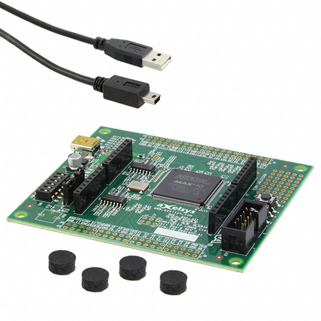
MAX 10 FPGA Evaluation Kit (Source: DigiKey)
Typical Application Areas
- Industrial Automation: PLC I/O expansion, motor control, sensor hub with on-chip ADC
- IoT Edge Computing: Protocol bridging (SPI/I²C/UART to Ethernet), edge inference co-processor
- Automotive-Adjacent: ADAS sensor preprocessing, CAN/LIN gateway, LED driver controller
- Test & Measurement: Data acquisition with dual 12-bit ADC, signal conditioning
- Video & Display: LVDS display interface controller, video overlay generator
- Communications: SDR front-end, protocol converter, custom serial interface
Video Tutorial: Getting Started with MAX 10 FPGA
Ready to start your next FPGA project? Check availability and pricing for the 10M16SAU169I7G and other MAX 10 variants at the wwdparts online store.
Frequently Asked Questions
What is the 10M16SAU169I7G and what family does it belong to?
The 10M16SAU169I7G is a non-volatile FPGA from the Altera (Intel) MAX 10 family. It features 16,000 logic elements, an integrated dual 12-bit ADC, and flash-based configuration memory in a 169-ball UBGA package. The "I7G" suffix indicates industrial temperature range (−40 °C to +100 °C) and speed grade 7.
Does the 10M16SAU169I7G require an external configuration memory?
No. The MAX 10 family uses internal flash-based configuration, providing true instant-on operation without an external EEPROM or flash chip. The device supports dual-image configuration for safe remote updates with automatic fallback to a known-good image.
What are the ADC specifications of the 10M16SAU169I7G?
The 10M16SAU169I7G integrates two independent 12-bit ADC blocks, each capable of up to 1 MSPS (mega-samples per second). Each ADC block supports up to 18 analog input channels through an internal multiplexer. The ADC operates from a dedicated analog supply and includes an internal voltage reference.
What package and I/O count does the 10M16SAU169I7G offer?
The device comes in a 169-ball UBGA (Ultra-Fine-pitch Ball Grid Array) package measuring 11 × 11 mm with 0.8 mm ball pitch. It provides 130 user I/O pins supporting 3.3 V, 2.5 V, 1.8 V, and 1.5 V LVCMOS standards, as well as LVDS differential signaling.
What design software is required for the 10M16SAU169I7G?
The 10M16SAU169I7G is supported by Intel Quartus Prime Lite Edition, which is available as a free download. Quartus Prime provides synthesis, place-and-route, timing analysis, and programming support. The Lite edition includes full support for all MAX 10 devices without requiring a paid license.
What is the difference between 10M16SAU169I7G and 10M16SAU169C8G?
Both devices have the same logic capacity (16K LEs) and package (169-ball UBGA). The key differences are: the "I7G" variant operates across the industrial temperature range (−40 °C to +100 °C) at speed grade 7, while the "C8G" variant is rated for commercial temperature (0 °C to +85 °C) at speed grade 8 (faster). Choose the I7G for harsh-environment or outdoor applications.


